Download
1 / 8
90 likes | 200 Views
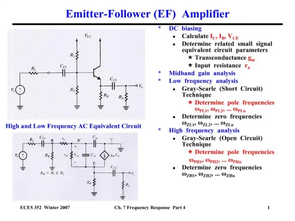
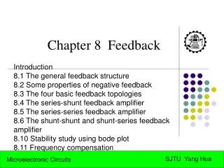
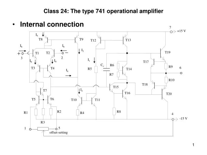
7. +15 V. I 5. T8. T9. T13. T12. I b. I b. I 3. T19. T2. T1. 2. 3. I 1. I 0. I 0. T17. C c. R6. R9. 6. T3. T4. R5. T14. I 4. R7. R10. T18. T15. I 2. T7. T16. T20. T6. T5. T10. T11. R2. R8. R1. R4. 4. -15 V. R3. 5. 1. offset-setting.

E N D
7 +15 V I5 T8 T9 T13 T12 Ib Ib I3 T19 T2 T1 2 3 I1 I0 I0 T17 Cc R6 R9 6 T3 T4 R5 T14 I4 R7 R10 T18 T15 I2 T7 T16 T20 T6 T5 T10 T11 R2 R8 R1 R4 4 -15 V R3 5 1 offset-setting Class 24: The type 741 operational amplifier • Internal connection
Class 24 • T12-R5-T11: input leg of 2 current mirrors • 0.7 mA • T11-T10 and T9-T8 CMs set the op point current of the input differential amplifier • 15μA - 15 μA • T12-T13 CM sets the oppoint current of the CE amplifier with a Darlington (and T14) • 0.7 mA • Class of the power amplifier is set by the 2VBcircuit of T14: 2VB= 0.96 Vclass AB
Class 24 • Side calculations: • For T1 and T2: ß ~ B = 15 000/100 = 150 • For T3 and T4 (lateral): B = 5 ! • AC operation: • Input differential amplifier • Complementary Cascode arrangement • Phase addition by T5–T6–T7 imp. CM • Trans-conductance GA1=2g21(1)/4=0.29mS • Input resistance Rind 4(1 + ß)rE1Mohm
Class 24 • Input differential amplifier (cont’d) • Output resistance (g22 = 0): Rout1= ∞ • CMRR is very high (according to the catalogue CMRR = 70 …90 dB). • Offset-setting • Main amplifier • The RC and RL of the CE stage • Input resistance: • Rin2=2h11(15)=2·100h11(16)=2·100·100·26/0.7=740 k
Class 24 • Voltage gain of the input stage • Av1d = GA1Rin2=0.29·740=215 • Voltage gain of the main amplifier (Rp~50k) • Av2= -(g21(16)/2)50 = - [(0.7/26)/2]50 = - 673 • The voltage gain of the power stage is practically Av3 1, the total differential gain of the entire operational amplifier: • Avd = Av1dAv2Av3 = 215 . 673 = 145 000 • From catalogue: Avd = 20 000 … 200 000
Avd, dB 106 -20dB/D fA1 = 1 M 0 5 f, Hz -40dB/D Class 24 • Frequency response • Miller-effect: Cd*=(1 + 673)30 = 20220 p • Resistive component:Rin2 • ωd=1/20220·10-12740·103=67 r/s, (fd=10Hz) • Cat: 5-10 Hz • Bode-plot
Class 24 • Slew rate (SR) • SR = (Vout/t)max = VC(T16)/t = =(iout1maxt)/(Cct) = Iout1max/Cc = =30A/30pF = 106V/s = 1V/s • Cat: 0.5V/s • Large signal limit frequency • lslVout p max=SR lsl=106/10=105 r/s • flsl=10kHz
Class 24 • Power amplifier • Current limiting(made by RE=R9=R10=25 ohm) • iout max =0.4V/25 ohm=16 mA • Output resistance:Rout=25+RB/h2175ohm • Maximum output voltage swing • vout p max=VS-2VBE–iout maxRE=15-2·0.6-0.4=13.4V • Linearity range: • vout p maxlin=10...12V