Download
1 / 13
130 likes | 307 Views
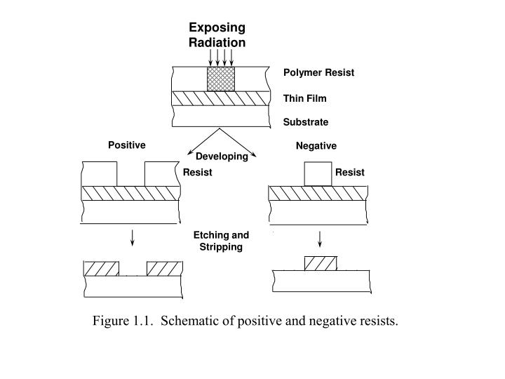
Exposing Radiation. Polymer Resist. Thin Film Substrate. Positive. Negative. Developing. Resist. Resist. Etching and Stripping. Figure 1.1. Schematic of positive and negative resists. D 0 –Threshold Dose. 1. Resist Film Thickness Remaining after Development. 0. D C –Clearing

E N D
Exposing Radiation Polymer Resist Thin Film Substrate Positive Negative Developing Resist Resist Etching and Stripping Figure 1.1. Schematic of positive and negative resists.
D0 –Threshold Dose 1 Resist Film Thickness Remaining afterDevelopment 0 DC –Clearing Dose Log Exposure Dose Figure 1.2.a. Characteristic curve of a hypothetical positive tone resist. b) optical projection lithography schematic.
source condenser Cr on glass mask reduction optics image in resist on wafer Figure 1.2.b. Optical projection lithography schematic.
Original gate pattern PSM regular mask image Figure 1.3.a. Dual-mask PSM technique. The original pattern for the gate is modified to create a phase shift mask and a “trim” mask. The phase shift mask creates a thin line exposure and the trim mask defines the remaining features.
Figure 1.3.b. SEM micrograph of DSP chip with 120 nm gates printed with 248nm DUV lithography and dual-mask PSM technique. The original gate size was 250 nm.
1974 1978 1990 SEM Gaussian Shaped Beam Cell/Character Increasing Throughput Figure 1.4. Gaussian beam, shaped beam, and cell projection DWEB schematics.
IMAGE IN RESIST Figure 1.5. Schematic of Electron Projection Lithography employing scattering contrast.
Figure 1.7. Atomic force microscope image of topography in PMMA following FIB exposure at 1pA beam current and a total irradiation time of 20 s per feature. (From Ref. 24 by permission of American Institute of Physics.)
Figure 1.8.a. Variation of feature size with distance of sample from focus position in FIB. (From Ref. 23 by permission of American Institute of Physics.)
Figure 1.8.b. FIB-induced Pt deposition onto the periphery of a 5 cm radius of curvature gold-coated glass lens, corresponding to height differences of order 30 m. All images and patterns are recorded without refocusing of the ion beam. Sub 100 nm resolution is maintained over the entire field.
a b c d e Figure 1.9. Schematic illustration of the microcontact printing process. (From Ref. 31 by permission of Elsevier.)
Figure 1.10. Schematic of nanoimprinting lithography process. (From Ref. 37 by permission of American Institute of Physics.)