Download
1 / 13
130 likes | 272 Views
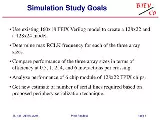
Simulation Study Goals. Use existing 160x18 FPIX Verilog model to create a 128x22 and a 128x24 model. Determine max RCLK frequency for each of the three array sizes. Compare performance of the three array sizes in terms of efficiency at 0.5, 1, 2, 4, and 6 interactions per crossing.

E N D
Simulation Study Goals • Use existing 160x18 FPIX Verilog model to create a 128x22 and a 128x24 model. • Determine max RCLK frequency for each of the three array sizes. • Compare performance of the three array sizes in terms of efficiency at 0.5, 1, 2, 4, and 6 interactions per crossing. • Analyze performance of 6 chip module of 128x22 FPIX chips. • Get new estimate of number of serial lines required based on proposed periphery serialization technique. Pixel Readout
Max RCLK • Created a worst case pattern for vertical token passing: hit in top pixel and hit in bottom pixel in same BCO and same column. • A setup violation occurs if the period of RCLK is less than the time it take the token to be released from the top pixel to the time it gets to the bottom pixel. Pixel Readout
Input Files • Dave provided input files (pixel hits) for 0.5, 1.0, 2.0, 4.0, and 6.0 interactions per crossing. Pixel Readout
Results Pixel Readout
Results Pixel Readout
6 Chip Module Simulation • Dave provided input files (pixel hits) for Chips 1, 2, 3, 4, 5, and 6 at 6 interactions per crossing. Pixel Readout
6 Chip Module Input Hits Summary Pixel Readout
Pixel Readout • Send two CLKs to each FPIX module • CLKA & CLKB are of same frequency but 90deg out of phase. Pixel Readout
Serialization Technique • Periphery serialization BW equals the peak data rate out of the core….no need for buffering (never any data loss in periphery) or data compression. • Set the core clock frequency (RCLK) so that the core peak data rate equals the serializer(s) BW. RCLK will be fast (34.72Mhz max) for hot chips, and slow for cold chips. Possible FPIX Periphery w/ single serial line Pixel Readout
Serialization FPIX Periphery w/ 2 serial lines and 3 serial lines Pixel Readout
Serialization FPIX Periphery w/ 6 serial lines Pixel Readout
Serialization • Assuming max RCLK frequency allowed is 34.72Mhz and max number of serial lines allowed is 6….serialization clock must be 34.72Mhz * 5 = 173.6Mhz. Pixel Readout
Module Efficiency at 6 Interactions/Crossing (3x Nominal) Pixel Readout