Download
1 / 54
540 likes | 612 Views
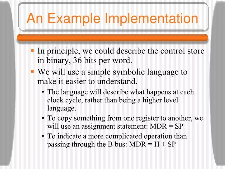
An Example Implementation. In principle, we could describe the control store in binary, 36 bits per word. We will use a simple symbolic language to make it easier to understand. The language will describe what happens at each clock cycle, rather than being a higher level language.

E N D
An Example Implementation • In principle, we could describe the control store in binary, 36 bits per word. • We will use a simple symbolic language to make it easier to understand. • The language will describe what happens at each clock cycle, rather than being a higher level language. • To copy something from one register to another, we will use an assignment statement: MDR = SP • To indicate a more complicated operation than passing through the B bus: MDR = H + SP
An Example Implementation • We must use only legal combinations in the assignment statement (e.g. no H = H - MDR). • We can assign the result to multiple registers, so we can also write: SP = MDR = SP + 1 • To indicate memory reads and writes of 4-byte data words, we will just put rd and wr in the microinstruction. • Fetching a byte through the 1-byte port is indicated by fetch. • Assignments and memory operations can occur in the same cycle. This is indicated by writing them on the same line.
An Example Implementation • Remember that each microinstruction must explicitly supply the address of the next microinstruction. • To ease the programmer’s job, the microassembler normally assigns an address to each microinstruction (not necessarily consecutive in the control store) and fills in the NEXT_ADDRESS field so that microinstructions written on consecutive lines are executed consecutively. • Sometimes, however, the programmer wants to branch away unconditionally: goto label.
An Example Implementation • To do a conditional branch, we can use the Z and N flip-flops: Z = TOS tests the TOS register to see if it is zero. • We can then do: Z = TOS; if (Z) goto L1; else goto L2 • Note that L2 must be exactly 256 more than L1 (the previous instruction causes Z to be ORed into the high-order bit of MPC). • To use the JMPC bit: goto (MBR OR value). This tells the microassembler to use value for NEXT_ADDRESS and set the JMPC bit so that MBR is ORed into MPC with NEXT_ADDRESS.
An Example Implementation • If value is 0, which is the normal case, we can just write: goto (MBR) • The actual microprogram that interprets IJVM is 112 microinstructions long. • Consecutive microinstructions are not necessarily located in consecutive addresses in the control store. • Note the meanings of the registers: • CPP is a pointer to the constant pool. • LV is a pointer to the local variables. • SP is a pointer to the top of the stack. • PC holds the address of the next instruction.
An Example Implementation • MBR is a 1-byte register that holds the bytes of the instruction stream as they come in to be executed. • At the beginning and end of each instruction, TOS contains the value of SP. For some instructions, POP for example, more work is necessary. • The OPC register is a temporary register. • The main loop of the interpreter begins on the line labeled MAIN1 and is a single microinstruction.
An Example Implementation • Control store addresses corresponding to opcodes must be reserved for the first word of the corresponding instruction interpreter. • Assume that MBR contains 0x60 (IADD). The main loop must: • Increment the PC, leaving it containing the address of the first byte after the opcode. • Initiate a fetch of the next byte into MBR. • Perform a multiway branch to the address contained in MBR at the start of Main1. This address is the opcode currently being executed.
Increasing the Speed • In general, we trade off speed versus cost. A faster implementation requires more hardware complexity. • There are three basic approaches for increasing the speed of execution: • Reduce the number of clock cycles needed to execute an instruction. • Simplify the organization so that the clock cycle can be shorter. • Overlap the execution of instructions.
Increasing the Speed • As another speed increase, notice that for every instruction the following operations may occur: • The PC is passed through the ALU and incremented • The PC is used to fetch the next byte in the instruction stream. • Operands are read from memory. • Operands are written to memory. • The ALU does a computation and the results are stored back. • We can free up the ALU by introducing an IFU (Instruction Fetch Unit).
The Mic-2 • The Mic-2, shown on the next slide • Incorporates the Instruction Fetch Unit (IFU) • This results in changed (smaller) microprogram to implement IJVM (at the expense of more hardware) for the IFU (which is implemented in hardware) • Has the new MBR2 16-bit register • Allows any register to be used as either operand (this simplifies the microprogram as well)
Pipelining • We can further speed up processing by overlapping the execution of the instructions. • In order to do this, we must break up the data path into three parts. • This is done by inserting latches (registers) in the data path. • Each of these parts executes faster than the original data path.
Pipelining in Mic-3 • In the Mic-3 shown on the next slide, latches have been inserted to allow each of the three components (Drive A and B bus, perform ALU computation, writeback result) to perform concurrently • Along with the IFU, this gives us a 4 stage pipeline
Pipelining • The operation of the pipeline is shown on the next slide • Note that several instructions are operating concurrently
Pipelining in Mic-4 • The following slide shows the Mic-4 in which several more stages are added • The decoding unit finds the microprogram memory location of the next opcode • The queueing unit receives the micro-op index from the decoding unit and copies the corresponding micro-op to a queue it continues copying micro-ops until last one in sequence • Separate MIRs for the several phases
Cache Memory • The recent improvements in CPU speed have led to an even wider gap between CPU and memory speeds. • One way to try to manage this problem is through the use of high-speed cache memory. • One technique that is quite efficient involves the use of a separate cache for memory and instructions. This is called a split cache.
Cache Memory • A split cache allows memory operations to be initiated independently in each cache, doubling the bandwidth of the memory system. • Each cache has independent access to the main memory. • An additional cache, called level 2 cache, may reside between the instruction and data caches and main memory. • There may be three or more levels of cache as more sophisticated memory systems are required.
Cache Memory • The following slide shows a typical arrangement. • The CPU chip itself contains a small instruction cache and a small data cache, typically 16 KB to 64 KB. • The level 2 cache is not on the CPU chip, but may be included in the CPU package, connected by a high-speed data path. • This cache is generally unified (containing both data and instructions) and is between 512 KB and 1 MB.
Cache Memory • The third level cache is on the processor board and contains a few megabytes of SRAM, which is faster than the main DRAM memory. • Caches are generally inclusive, with the full contents of the level 1 cache being in the level 2 cache and the full contents of the level 2 cache being in the level 3 cache.
Cache Memory • Cache memories depend on two kinds of address locality to achieve their goal. • Spatial locality is the observation that memory locations with addresses numerically similar to a recently accessed location are likely to be accessed. • Temporal locality occurs when recently accessed memory locations are accessed again. • Main memory is divided into fixed-size blocks called cache lines of 4 to 64 bytes. • Lines are numbered consecutively starting at 0, so with a 32-byte line size, line 0 is bytes 0 to 31, etc.
Cache Memory • At any instant, some lines are in the cache. • When memory is referenced, the cache controller circuit checks to see if the word referenced is currently in the cache. • If it is, it is used. • If not, some line entry is removed from the cache and the line needed is fetched from memory or some lower level cache to replace it. • Many variations exist, but the central idea is always to keep the most heavily-used lines in the cache.
Cache Memory • Cache memory can be organized several ways: • Direct-mapped caches fix the cache entry in which a particular portion of main memory can be stored. This is the fastest kind of cache to search, but the most inflexible. • Set-associative caches allow a portion of main memory to be stored in one of several cache entries. This allows fast retrieval and flexible storage. • A fully-associative cache allows memory to be stored in any entry of the cache. Retrieval is very slow, so this organization is not very practical.
Direct-Mapped Caches • Direct mapped caches contain a number (say 2048) of entries. Each entry consists of: • The Valid bit which indicates whether there is any valid data in this entry or not. Initially, all entries are marked invalid. • The Tag field consists of a unique value (in the example, 16 bits) identifying the corresponding line of memory from which the data came. • The Data field contains a copy of the data in memory. This fields holds one cache line of 32 bytes.
Direct-Mapped Caches • A memory word can be stored in exactly one place within a direct-mapped cache. • Given a memory address, there is only one to place to look for it in the cache. • For storing and retrieving data from the cache, the address is broken into 4 components: • The TAG field corresponds to the Tag bits stored in a cache entry. • The LINE field indicates which entry holds the corresponding data, if they are present.
Direct-Mapped Caches • The WORD field tells which word within a line is referenced. • The BYTE field is usually not used, but if only a single byte is requested, it tells which byte within the word is needed. For a cache supplying only 32-bit words, this field will always be 0. • When the CPU produces an address, the hardware extracts the 11 LINE bits from the address and uses these to index into the cache to find one of the 2048 entries. • If the entry is valid, the tags are compared, if they agree, a cache hit has occurred.
Direct-Mapped Caches • If the cache entry is invalid or the tags do not match, a cache miss has occurred. • In this case, the 32-byte cache line is fetched from memory and stored in the cache entry, replacing what was there. • If the existing cache entry has been modified since being loaded, it must be written back to main memory. • The retrieval process is made faster by performing the retrieval from the cache in parallel with the comparison of the tags.
Direct-Mapped Caches • Up to 64K bytes of contiguous data can be stored in the cache. • However, two lines that differ by a multiple of 64K (65,536 bytes) cannot be stored in the cache at the same time. • Direct-mapped caches are the most common kind of caches, and they perform quite well since collisions of the kind described above don’t happen often. • A compiler can take the cache into account when placing data and instructions in memory.
Set-Associative Caches • A solution to the problem of lines competing for the same cache entry is to allow two or more lines in each cache entry. • A cache with n possible entries for each address is called an n-way associative cache. • A set associative cache is inherently more complicated than a direct-mapped cache because we need to check up to n tags to see if the needed line is present in an entry. • Two-way and four-way caches perform quite well.
Set-Associative Caches • The use of a set-associative cache brings up the question of which line should be discarded when a new line is brought into the entry. • A good choice is to use the LRU (Least Recently Used) algorithm which replaces the line which was accessed longest ago. • If we carry the set-associative idea to the extreme, we have a 2048-way cache or a fully-associative cache. These don’t improve much over the performance of 4-way caches and so are not much used.
Cache Policy • Writing a word of memory in the cache causes a problem we can use • Write through (immediately update main memory) • Write back (only update main memory when cache line is evicted) • Further we need to decide whether to use write allocation (should we bring a cache line into memory when we write an uncached line?) • Good for write back, not for write through
Branch Prediction • Modern computers are highly pipelined, having up to 10 or more stages. • Pipelining works best on linear code, so consecutive words from memory can be read and sent off to be executed. • Unfortunately, real code is full of branches. • See, for example, the code of the next slide. • Two of the five instructions are branches, and the longest linear code sequences here is two instructions.
Branch Prediction • Even unconditional branches cause problems since we have to decode the instruction (in the pipeline) to see that the instruction is a branch. • A number of pipelined machines (such as the UltraSPARC III) have the property that the instruction following an unconditional branch is executed, though logically it should not be. • The position after a branch is called a delay slot. • The Pentium 4 does not have this property, but this adds complexity. The compiler tries to put a useful instruction or NOP after the branch.
Branch Prediction • Conditional branches are even worse since not only do they have delay slots, but now the fetch unit does not know where to read from until much later in the pipeline. • Early pipeline machines just stalled until it was known whether the branch would be taken or not. • What most machines do now when they hit a conditional branch is predict whether it will be taken or not. • One technique: assume all backward branches are taken and forward ones are not.