Download
1 / 32
330 likes | 567 Views
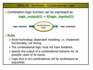
Synthesis of Combinational Logic. Lab 1 due tonight, Quiz 1 during Friday’s recitation. Boolean Minimization: An Algebraic Approach. Approach: repeated application of For any expression α and variable A: This is the basis for most software simplification approaches –

E N D
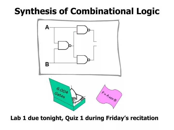
Synthesis of Combinational Logic Lab 1 due tonight, Quiz 1 during Friday’s recitation
Boolean Minimization:An Algebraic Approach Approach: repeated application of For any expression α and variable A: This is the basis for most software simplification approaches – e.g., Quine-McClusky reduction. Hmmm… Can’t we re-write The truth table To make “mergeable” Terms more obvious?
Karnaugh Maps: A Geometric Approach K-Map: a truth table arranged so that terms which differ by exactly one variable are adjacent to one another so we can see potential reductions easily. It’s cyclic. The left edge is adjacent to the right edge. (It’s really just a flattened out cube). Here’s the layout of a 3-variable K-map filled in with the values from our truth table:
On to Hyperspace 4-variable K-map for a multipurpose logic gate: Again it’s cyclic. The left edge is adjacent to the right edge, and the top is adjacent to the bottom.
Finding Subcubes We can identify clusters of “irrelevent” variables by circling adjacent subcubes of 1s. A subcube is just a lower dimensional cube. The best strategy is generally a greedy one. • Circle the largest N-dimensional subcube (2N adjacent 1’s) • Continue circling the largest remaining subcubes (even if they overlap previous ones). • Circle smaller and smaller subcubes until no 1s are left.
Write Down Equations Write down a product term for the portion of each cluster/subcube that is invariant.
Recap: K-map Minimization • Copy truth table into K-Map • Identify subcubes, selecting the largest available subcube at each step, even if it involves some overlap with previous cubes, until all ones are covered. (Try: 4x4, 2x4 and 4x2, 1x4 and 4x1, 2x2, 2x1 and 1x2, finally 1x1) • Write down the minimal SOP realization
Are K-maps Really all that Useful? • They are only manageable for small circuits (4-5 inputs at most) • Sometimes you pick the wrong set of subcubes • There are better techniques (better for computers, not us) • SOP realizations aren’t all that relevant • We’ve got gates to burn • Low fan-in gates are better suited to current technologies that SOP (FPGAs, Standard Cells) • Sometimes minimal circuits are glitchy • Some important circuits aren’t amenable to minimal SOP realizations
Logic that defies SOP simplification Can simplify the carry out easily enough, eg... Co = BC + AB + AC But, the sum, S, doesn’t have a simple sum-of-products implementation even though it can be implemented using only two 2-input gates.
Systematic Implementation ofCombinational Logic Consider implementation of some arbitrary Boolean function, F(A,B) ... using a MULTIPLEXER as the only circuit element:
General Table Lookup Synthesis Generalizing: In theory, we can build any 1-output combinational logic block with multiplexers. For an N-input function we need a 2N input mux. BIG Multiplexers? How about 10-input function? 20-input?
A Mux’s Guts Multiplexers can be partitioned into two sections. A DECODER that identifies the desired input,and a SELECTOR that enables that input onto the output. Hmmm, by sharing the decoder part of the logic MUXs could be adapted to make lookup tables with any number of outputs
A New Combinational Device NOW, we are well on our way to building a general purpose table-lookup device. We can build a 2-dimensional ARRAY of decoders and selectors as follows ...
Shared Decoding Logic We can build a general purpose “table-lookup” device called a Read-Only Memory (ROM), from which we can implement any truth table and, thus, any combinational device Made from PREWIRED connections , and CONFIGURABLE connections that can be either connected or not connected
ROM Implementation Technology PFET with gate tied to ground = resistor pullup that makes wire “1” unless one of the NFET pulldowns is on. Hardwired AND logic Programmable OR logic Advantages: - Very regular design (can be entirely automated) Problems: - Active Pull-ups (Static Power) - Long metal runs (Large Caps) - Slow JARGON: Inputs to a ROM are called ADDRESSES. The decoder’s outputs are called WORD LINES, and the outputs lines of the selector are called BIT LINES.
Speeding up ROMS The key to making ROMS go fast is to minimize the capacitances of those long wires running through the array. The best way to accomplish this is to build square arrays:
Logic According to ROMs ROMs ignore the structure of combinational functions ... • Size, layout, and design are independent of function • Any Truth table can be “programmed” by minor reconfiguration: • Metal layer (masked ROMs) • Fuses (Field-programmable PROMs) • Charge on floating gates (EPROMs) ... etc. Model: LOOK UP value of function in truth table... Inputs: “ADDRESS” of a T.T. entry ROM SIZE = # TT entries... ... for an N-input boolean function, size = 2N x #outputs Why do ROM SIZES grow by factors of 4?
Example: 7-sided Die What nature can’t provide… electronics can (with the magic of LEDs!). We want to construct a readout displaying the following symbols: An array of LEDs, labeled as follows, can be used to display the outcome of the die:
ROM-Based Design Once we’ve written out the truth table we’ve basically finished the design Possible optimizations: • Eliminate redundant outputs • Addressing tricks
A Simple ROM implementation That was easy but there is clearly some waste. • unused products • over-specified terms
Another General-Purpose Logic Device What if the AND terms of a ROM’s decoder were programmable in the same way that the OR terms are? Then we could use some of our logic minimization tricks to reduce the size of the ROM array. PLA – Programmable Logic Array
PLA 7-sided Die implementation PLAs like ROMs support the synthesis of arbitrary logic functions using SOP implementations. However, they allow for • minimal realizations • smaller (faster) arrays Regular structure • automatic generation • easy design • still slower than optimized gates
PALs: Programmable Array Logic Another approach to structured logic design is Programmable Array Logic (PAL). These were once popular off-the- shelf devices. They basically replaced TTL gates in the ‘80s and fueled the minicomputer revolution. Today, they are practically fossils PALs have a programmable decoder (AND plane) with fixed selector logic (OR plane). These devices were useful for implementing large fan-in gates and SOP logic expressions. They could be purchased as unprogrammed chips and configured in the field using an inexpensive programmer.
Standard Cells First, a library of fixed-pitch logic cells (gates, registers, muxes, adders, I/O pads, …) are created. A data sheet for each cell describes its function, area, power, propagation delay, output rise/fall time as function of load, etc.
Standard Cell Example Similar to designing with board level components 20 years ago. CAD tools place and route cells. • minimize area • meet timing specs In this case, the router needed so much space for running wires that cell rows were pushed apart. In many cases, wiring determines the size of the layout!
Fast Turn-around: Gate Arrays Gate arrays use fixed arrays of transistors that are “personalized” in a final processing step that adds wires and contacts. Most popular architecture is “Sea-of- Gates” where the core of the chip is a continuous array of FETs. Routing occurs over the top of unused transistors. Pros: • can be prefabricated • only last few masks are customized
Gate Array Example The last two layers of metal are used to define the function of the transistors. Side-by-side gates are isolated from one another by turning off the gate of a transistor between them. This is called “gate-isolation.”
Summary • Sum of products • Karnaughmaps • Use minimal cover of prime implicants to get minimal SOP • Use all prime implicants to get lenient (glitch-free) implementation • Primitive, manual version of logic optimization algorithms • SOP implementation methods • NAND-NAND, NOR-NOR • Muxes used to build table-lookup implementations • ROMs • Decoder logic generates all possible product terms • Selector logic determines which p’terms are or’ed together • PLAs are ROMs with optimized decoders that generate only the product terms that are needed