Download
1 / 78
780 likes | 787 Views
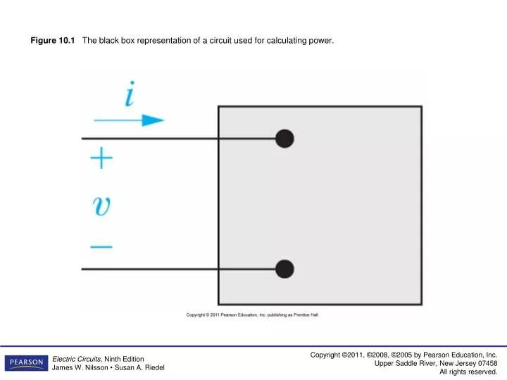
Figure 10.1 The black box representation of a circuit used for calculating power. Figure 10.2 Instantaneous power, voltage, and current versus v t for steady-state sinusoidal operation. Figure 10.3 Instantaneous real power and average power for a purely resistive circuit.

E N D
Figure 10.1 The black box representation of a circuit used for calculating power.
Figure 10.2 Instantaneous power, voltage, and current versus vt for steady-state sinusoidal operation.
Figure 10.3 Instantaneous real power and average power for a purely resistive circuit.
Figure 10.4 Instantaneous real power, average power, and reactive power for a purely inductive circuit..
Figure 10.5 Instantaneous real power and average power for a purely capacitive circuit.
Figure 10.7 A sinusoidal voltage applied to the terminals of a resistor.
Figure 10.8 The effective value of s (100 V rms) delivers the same power to R as the dc voltage Vs (100 V dc).
Figure 10.11 The phasor voltage and current associated with a pair of terminals.
Figure 10.12 The general circuit of Fig. 10.11 replaced with an equivalent impedance.
Figure 10.15 (a) The power triangle for load 1. (b) The power triangle for load 2. (c) The sum of the power triangles.
Figure 10.16 (a) The sum of the power triangles for loads 1 and 2. (b) The power triangle for a 424.4 µF capacitor at 60 Hz. (c) The sum of the power triangles in (a) and (b).
Figure 10.19 The circuit shown in Fig. 10.18, with the network replaced by its Thévenin equivalent.
Figure 10.21 A simplification of Fig. 10.20 by source transformations.
Figure 10.22 The circuit shown in Fig. 10.20, with the original network replaced by its Thévenin equivalent.
Figure 10.26 The circuit used to calculate the short circuit current.
Figure 10.27 The Thévenin equivalent loaded for maximum power transfer.
Figure 10.28 Schematic representation of a handheld hair dryer.
Figure 10.30 (a) The circuit in Fig. 10.29 redrawn for the LOW switch setting. (b) A simplified equivalent circuit for (a).
Figure 10.31 (a) The circuit in Fig. 10.29 redrawn for the MEDIUM switch setting. (b) A simplified equivalent circuit for (a).
Figure 10.32 (a) The circuit in Fig. 10.29 redrawn for the HIGH switch setting. (b) A simplified equivalent circuit for (a).