Download
1 / 43
430 likes | 549 Views
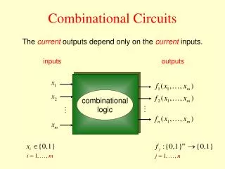
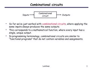
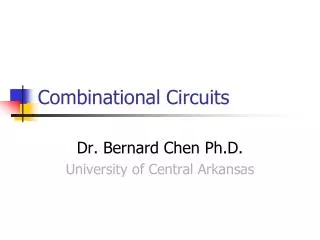
Combinational circuits. Changes at inputs propagate at logic speed to outputs Not clocked No internal state (memoryless). 1. Example. O. I. I0. &. 1. O. I1. &. I2. D Q. NOT combinational. &. &. S R - latch (has a state). D - flip-flop (clocked, no path). 1. 1. 1.

E N D
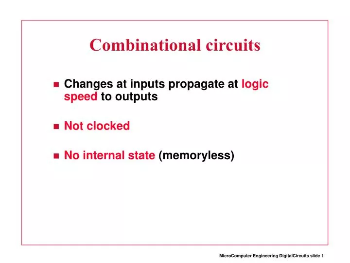
Combinational circuits • Changes at inputs propagate at logic speed to outputs • Not clocked • No internal state (memoryless)
1 Example O I I0 & 1 O I1 & I2
D Q NOT combinational & & S R - latch (has a state) D - flip-flop (clocked, no path)
1 1 1 1 1 1 1 1 Combinational logic - can be connected into sequences - can be connected parallel &
1 1 1 1 1 1 Combinatorial loop This is OK: But what is this?
1 1 1 Combinationial loop 0 1 1 0 Impossible! Logical nonsense Electrical trouble
1 1 1 Combinational loop This is a “combinational loop” We must never have, or form, a combinational loop
D Q How is this usually solved? “The edge-triggered flip-flop!”
D Q The edge-triggered flip-flop! • Never a combinational path from in to out • A memory device, holds the value of “Q” until “clocked” • Ignores the value at “in” until “clocked” in out
D Q Beginners explanation • Flipflop “samples” its input at the rising edge and presents that value on the output. t 1 clock 0 A “rising edge” A “falling edge”
D Q Flip flops in the circuit We will put flip flops in our circuit (Good for “breaking” combinational loops) and clock them all with the same clock
Timing of a positive edge triggered D flip-flop • Setup time, tsetup the time the D input must be stable before the rising edge of the flip-flop. • Hold time, thold the time the D input must be stable after the rising edge of the clock D Clk Q 1, 0 or metastable! t t setup hold If the setup or hold time parameters are violated the Q output will be either logic 0, logic 1 or the flip-flop will enter a metastable state, but will eventually become a valid logic level.
D Clk Q 1, 0 or metastable! t t t hold pLH(CQ) pHL(CQ) t setup Clock to output delay • Clock-to-output delay, tpThe delay of a low to high transition and the delay of a high to low transition may be different.
1 D Q 1 Example BAD OK Suppose the flip flop holds a “1”. Let’s clock this circuit...
D Q 1 Example 0 1 0 Holding Clock “pulse” one “clock cycle”
D Q 1 0 1 0 Example Samples the “0”
D Q 1 0 0 0 Example The exact instant that the output changes!
D Q 1 1 0 1 Example ... the circuit becomes stable again A very short time later... Called a logic “delay” (Propagation through the combinational logic)
D Q 1 1 0 1 Example ... until the next clocking And it stays like that....
Combinational logic in the MIPS • Zero extend box • Sign extend box • Controllable sign/zero extend box • “Tap box” (pick out fields of bits) • Shift left two bits
16 16 16 Zero extend box 16 zeroes ! Out[16..31] In[0..15] Out[0..15]
16 16 16 Sign extend box In[15] copied 16 times Out[16..31] In[0..15] Out[0..15]
16 16 16 Controllable zero / sign extend box Control & Out[16..31] In[15] In[0..15] Out[0..15]
6 5 32 5 5 16 Tap box • Contains no logic circuits • Regroup input bits Opcode field Rs field Instruction Rt field Rd field Immediate field
Shift left two bits Out bit [2..31*] 32 In bit [0..31] Out bit 1 0 Out bit 0 0 * Two bits lost
Arbitrary logic • Given a truth table: A B C D X Y Z 0 0 0 0 1 1 0 0 1 - 1 0 1 - - 1 1 0 1 0 1 • Digital design....... Logic A B C D X Y Z
So, it’s enough just to have the truth table..... We have tools to build the “logic box” “Logic synthesis”
The multiplexor • Special truth table: A B Cont Out 0 - 0 0 1 - 0 1 - 0 1 0 - 1 1 1 • Easy to generalise to “A, B, C, D....” A Out B Cont
"0" msb lsb "0" msb lsb "0" Shifters Two kinds: logical-- value shifted in is always "0" arithmetic-- on right shifts, sign extend Note: these are single bit shifts. A given instruction might request 0 to 32 bits to be shifted!
Example: 4 bit Logical Right Shifter A3 A2 A1 A0 ”0” S0 ”0” S1 If added Right-to-left connections could support Rotate (not in MIPS but found in ISAs)
A3 A2 A1 A0 ”0” S0 = 0 ”0” A3 A1 A2 A0 A3 ”0” A2 S1 = 1 Example: 4 bit logical Right Shifter II • Shift two bits right
Example: 4 bit Right Shifter III A3 A2 A1 A0 ”0” S0 = 0 ”0” A3 A1 A2 A0 A3 ”0” A2 S1 = 1 ”0” ”0” A3 A2 If added Right-to-left connections could support Rotate (not in MIPS but found in ISAs)
S 0 (0,1) S 1 (0, 2) S 2 (0, 4) S 3 (0, 8) General Shift Right Scheme 16 bit using MUXes If added Right-to-left connections could support Rotate (not in MIPS but found in ISAs)
SR3 SR2 SR1 SR0 D3 D2 A2 D1 A1 D0 A0 A3 A2 A1 A0 BarrelShifter (remember?) Technology-dependent solutions: 1 transistor per switch:
32 32 32 What about adders? A[0] A[1] .... A[31] B[0] ....... B[31] C[0] C[1] .... C[31] • Impractical to represent by truth table • Exponential in number of input bits A + C B
Adders are special ..... • We’ll talk about them later • Also, multipliers • Let’s just assume they exist
32 32 32 1 32 32 32 Subtract ? A - B ? = A + NOT (B) + 1 Yes, there’s an easier way... A + 32 B + 1
Controllable Add / Sub ? A B Add Subtract Choose
32 A 32 + 32 32 B =1 Carry in Choose How it’s really done
32 32 32 What’s the point of this ? • The ALU is combinational • Must have control signals to choose! ALU Control points
1 1 1 1 1 32-bit wide inverter ? Out bit[31] In bit[31] Out bit[30] In bit[30] Out bit[1] In bit[1] Out bit[0] In bit[0] 32 32 Easier to draw!
Same idea : • 32 - bit wide multiplexors • 32 - bit wide clocked registers, such as the • Program counter • write back data register 32 32 D Q Clock signal not drawn
Memories ? • Register file • Instruction memory • Data memory • We’ll treat these as combinational (not “clocked”)