Download
1 / 13
130 likes | 137 Views
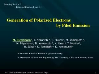
Morning Session II -- Polarized Electron Beam II --. Generation of Polarized Electrons by Filed Emission. M. Kuwahara A , T. Nakanishi A , S. Okumi A , M. Yamamoto A , M. Miyamoto A , N. Yamamoto A , K. Yasui A , T. Morino A , R. Sakai A , K. Tamagaki A , K. Yamaguchi B.

E N D
Morning Session II -- Polarized Electron Beam II -- Generation of Polarized Electrons by Filed Emission M. Kuwahara A, T. Nakanishi A, S. Okumi A, M. Yamamoto A, M. Miyamoto A, N. Yamamoto A, K. Yasui A, T. Morino A, R. Sakai A, K. Tamagaki A, K. Yamaguchi B A: Graduate School of Science, Nagoya University B: Department of Electronic Engineering, The University of Electro-Communications PST'05 (XIth Workshop on Polarized Source and Target)
Motivation • Spin polarized electrons • Necessary for high energy physics • Linier collider project (ILC project) • Powerful application for material sciences • Spin electron microscopy (SP-LEEM, Spin-SEM, TEM, …) • Electron beam holography considered a spin effect • Photocathode developments by GaAs-GaAsP strained superlatttice • Polarization ~90% @QE 0.5% • Generation of multi-bunch beam (by overcoming SCL effect) • Few problems are still remained • Low emittance and long life time of photocathode • Low Emittance and High Brightness Polarized e- beam • Extraction of Polarized e- beam without NEA surface problem PST'05 (XIth Workshop on Polarized Source and Target)
Using tip-GaAs (the feature is needle like) Field emission from very small area of the top Method 1.Low emittance spin polarized electron [i] spin polarizing →GaAs type semiconductor [ii] low emittance →cross section of beam: very small 2.NEA surface lifetime problem (by avoiding NEA surface) Using a tunneling effect by a high gradient at the surface → Field Emission PST'05 (XIth Workshop on Polarized Source and Target)
Generation of spin polarized electrons Basis of generating spin polarized electrons Under illuminating circular light to GaAs semiconductor. Selective excitation from valence band to conduction band. (conserving the helicity) Left figure shows a principled basis that excitation process of spin polarized electrons in GaAs semiconductor. By strained or super-lattice structure GaAs, the degeneracy at G point can be separated, Polarization > 50% enable In fact, Polarization ~ 90% by strained supper-lattice structure Bulk-GaAs has degeneracy of electron bands at G. Polarization: max. 50% PST'05 (XIth Workshop on Polarized Source and Target)
H3PO4:H2O2:H2O=10:1:1 Temperature 20℃ temperature H3PO4:H2O2:H2O=5:1:1 Temperature -1℃ ratio Photocathode ・Photocathodesample (GaAs tip) ・Fabrication of tip-GaAs (p-GaAs substrate, Zn-dope:2×1019cm-3) Height :~10mm Radius :~25nm SEM images (left:×25k, right:×100) H3PO4 etching solution’s condition, mixing ratio and temperature PST'05 (XIth Workshop on Polarized Source and Target)
Apparatus Electron gun • 70keV PES(I-V characteristics and polarization measurement) Mott-scattering polarization analyzer Vacuum pressure :3×10-11 Torr Field gradient at photocathode:0.6MV/m @70kV • 20kV DC-gun (I-V characteristics) 20kV-DCgun, variable gap separation Field gradient at photocathode ~ 4.8MV/m (@20kV, gap=3.2mm) Laser Ti:Sapphire Laser 20kV DC-gun 70keV PES PST'05 (XIth Workshop on Polarized Source and Target)
Experimental results (1) - I-V characteristics - • Behaviors ; under impressing high gradient and illuminating circular light I-V characteristic → F-N(Fowler-Nordheim) plot Tunneling effect through a surface barrier (Field emission) Not observe by GaAs without tip Field-Emission is observed Photon-excited electrons were extracted by F.E.mechanism QE vs. Photon energy at high gradient field ( E=3.4MV/m @Flat) well fit Fitting curve is estimated by WKB approximation. Demonstrated the tunneling yield depending on an excitation energy. PST'05 (XIth Workshop on Polarized Source and Target)
Estimation of electron affinity c [Estimation of c by the QE–l data] Assumption: proportional to a tunneling yield of surface barrier Tunneling yield T (WKB approximation) is written by The solid line is obtained by least-squares fitting in left figure. Therefore, c is estimated as →0.282 eV [Estimation of c by F-N plot data] F-N plot is written as, ←Fowler-Nordheim equation Consistent with each result By the gradient of F-N plot c=1.64×10⁻²b2/3 Here, field enhancement factor is 51 (calculated by POISSON) for the tip feature (curvature is 50nm, distance is 200mm) →0.226 eV PST'05 (XIth Workshop on Polarized Source and Target)
Experimental results (2) - Spin Polarization - • Polarization of tip-GaAs 1) Polarization :20~40% ≧Bulk-GaAs’ Polarization 2) tip-GaAs Polarization was higher than NEA/Bulk-GaAs’ at shorter wavelength l < 760nm (1.6eV) Corresponding with the rising edge of Q.E. We succeed in generation of spin polarized electrons by field emission ESP and QE spectrum under irradiating circular light. In order to compare, NEA/Bulk-GaAs polarization is also drown. Spin polarization did not get worse, while F.E. mechanism was substituted for NEA PST'05 (XIth Workshop on Polarized Source and Target)
Difference of each polarization • Generation process ①absorption and excitation ②diffusion and transport ③escape into vacuum • In transmission to the surface dependent on excitation energy (Phenomena of hot-electron) [1] Scattering in drifting process LO phonon scattering, impurity scattering [2] Spin flip in scattering BAP-process, DP-process, EY-process Spin relaxation time becomes smaller with rising electron energy Spin relaxation time 75~85ps (850to880nm), Band-gap 865nm(1.43eV) (different point between NEA and F.E.) PST'05 (XIth Workshop on Polarized Source and Target)
Difference of each polarization • Process in extracting into vacuum • Tunneling yield is sensitive to the excitation energy drifting electron: Energy dispersion becomes wider in transport process by some scattering. Polarization of higher energy part : High polarization lower energy part : Low polarization (cause by scattering) High energy part is mainly extracted into vacuum. ->Polarization becomes higher (cut off of depolarization part ) Surface tunneling is like a filter effect of polarization. Higher energy part of electrons can be extracted dominantly. De : narrow, Pol : high Fig. Generation process of spin polarized electrons with field emission. Blue color density means value of spin polarization. PST'05 (XIth Workshop on Polarized Source and Target)
Conclusion • Achievements : We demonstrated that F.E. can be used for PES as a substitute for using NEA surface. Probability of miniaturization, integration and applications for accelerators, microscopy, holography and so on. • Extraction of polarized electrons by F.E. : O.K. • Electrons extracted by F.E. have higher polarization. It is thought that filter effect of tunneling process in surface. • Lifetime (long lifetime compared with NEA surface (NEA~1week → F.E.>1month)) • Problem :Work function, fine structure, surface contamination • Stability and uniformity of current • Field emission characteristic (operation voltage, field enhancement) • Extract more high current We can confirm that spin polarized electrons can be extracted by F.E. , and demonstrate the fundamental characteristics. PST'05 (XIth Workshop on Polarized Source and Target)
Difference from NEA/Bulk-GaAs (2) • Depolarization effect of spin polarized electron in a GaAs crystal. (In the case of hot-electrons) • DP-process (>10meV) (p-dope>10^18 cm-3 , 10meV以下ではBAP機構が主たる効果) • LO phonon scattering. • SO splitting >341meV (in GaAs) Spin polarization of electrons diffusing into the surface (calculated by DP-process) PST'05 (XIth Workshop on Polarized Source and Target)