Download
1 / 22
220 likes | 232 Views
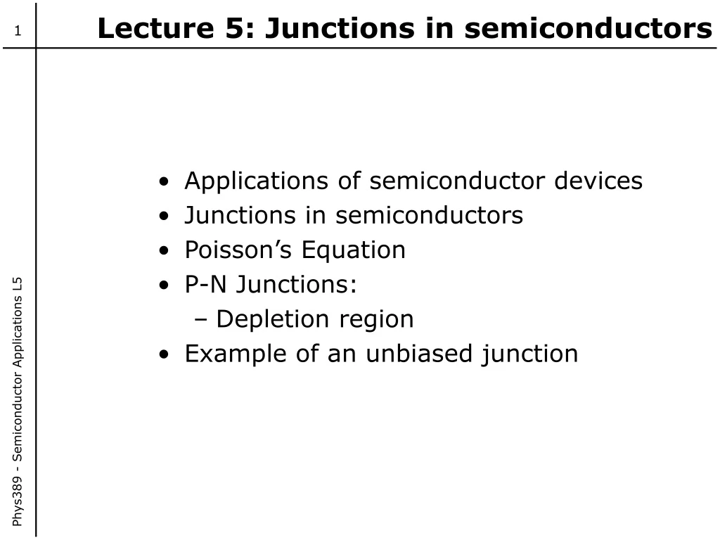
Lecture 5: Junctions in semiconductors. Applications of semiconductor devices Junctions in semiconductors Poisson’s Equation P-N Junctions: Depletion region Example of an unbiased junction.

E N D
Lecture 5: Junctions in semiconductors • Applications of semiconductor devices • Junctions in semiconductors • Poisson’s Equation • P-N Junctions: • Depletion region • Example of an unbiased junction Phys389 - Semiconductor Applications L5
How can our knowledge of the basic physical phenomena associated with semiconductors be exploited produce (understand) electronic devices? Modern devices are required to do: Information reception/detection: Semiconductor diodes, transistors and photo detectors serve the role of detecting signals of various kinds. Information amplification: Information received from a device may be weak – the signal must be amplified. Bipolar and field effect transistors are extremely useful devices because they are capable of large gain. Information manipulation: May involve addition, multiplication or logic decisions such as AND, OR etc. Specialist input/output relationships (high 1 or low 0 for digital applications). Devices must have high gain and a non-linear response. Device requirements: Shopping list Phys389 - Semiconductor Applications L5
Modern devices are required to: Store Information: Semiconductor memories based on transistors are much faster than magnetic tapes and disks. Rapid cost decreases in the former are increasing market share. Information Generation: Take a stream of incoming information and generate an outgoing stream of electronic or optical information. Microwave devices and semiconductor lasers are examples of semiconductor devices that are being used to generate information. Information Display: Semiconductor devices such as light-emitting diodes are important devices in the display market. Device requirements: Shopping list Phys389 - Semiconductor Applications L5
Electric properties of semiconductors can be altered by doping, however we have no ability to instantaneously alter the state of a device. If we can use the conductivity of the device, by rapidly changing its value we can define a state. An important requirement of good devices is non-linear response. The rectifying response is a good example, the flow is easy in one direction and difficult in the other. Semiconductors become useful when instead of having a uniform chemical composition, they have spatially non-uniform compositions. The idea of a junction is introduced. The most important junction is the p-n junction. The need for junctions Phys389 - Semiconductor Applications L5
Used as a device in applications as rectifiers, waveform shapers, lasers, detectors etc. It forms a key part of the bipolar transistor, one of the most important electronic devices. In a p-n junction the nature of the dopants is altered across a boundary to create a region that is p-type next to a region that is n-type. Questions: What are the carrier distributions for electrons and holes in the material? What are the physical processes responsible for current flow in the structure when a bias is applied? The P-N junction Phys389 - Semiconductor Applications L5
The unbiased P-N junction Phys389 - Semiconductor Applications L5
Three major regions can be identified: The p-type region: The material is neutral and the bands are flat. The density of acceptors balances the density of holes. The n-type region: Neutral material where the density of donor exactly balances the electron density. The depletion region: The bands are bent and a field exists that removes the mobile carriers, leaving negatively charged acceptors in the p-type region and positively charged donors in the n-type region. The depletion region, extends a distance Wp and Wn in the p and n regions respectively – an electric field exists. A drift current exists that counterbalances the diffusion current, which arises because of the difference in electron and hole densities across the junction. The unbiased P-N junction Phys389 - Semiconductor Applications L5
To describe the junction properties, knowledge of the width of the depletion region, the charge distribution of electrons and holes and the electric field is required. Analytical results can be obtained only if some simplifications are made: The physical junction is abrupt and each side uniformly doped. While the mobile charge density in the depletion region is not zero, it is much smaller than the background fixed charges. In order to solve the Poisson equations the assumption is the mobile carrier density is zero – called the depletion approximation. The transition between the bulk neutral n or p-type region and the depletion region is abrupt It is necessary us to identify all the current components flowing in the device The unbiased P-N junction Phys389 - Semiconductor Applications L5
There is an electron driftcurrent and electron diffusioncurrent as well as the hole drift and hole diffusion current. When there is no applied bias, these currents cancel each other individually. The hole current density is: The drift current density in the depletion region is really ep(x)vs(x) and independent of E, where vs is the saturated velocity. The field in the depletion region is very large even under equilibrium. The unbiased P-N junction Phys389 - Semiconductor Applications L5
The ratio of mp and Dp is given by the Einstein relation: As a result of bringing the p and n type semiconductors, a built-in voltage, Vbi is produced between the n and the p side of the structure. The built in potential is given by: Where n and p refer to the two sides of the junction. With a little rearrangement it can be shown that: The unbiased P-N junction Phys389 - Semiconductor Applications L5
If nn and np the electron densities in the n-type and p-type regions, the law of mass action (np = constant) says: Thus, the built in potential Vbi=Vn-Vp: The width of the depletion region can be determined once we have knowledge of the impurity concentration. In the depletion region, the mobile carrier density of electrons and holes is very small compared to the fixed background charge. The unbiased P-N junction Phys389 - Semiconductor Applications L5
For a p-n junction Poisson’sequation allows us to determine the value of the potential (r)at any point inside the diode. Where r(r) is the net charge density: n is the impurity concentration defined as the difference between the density of donors Nd and the density of acceptors Na. In one dimension: Now the shape of the potential across the junction can be obtained by twice integrating the charge distribution profile r(x). The diode as a detector Phys389 - Semiconductor Applications L5
The Poisson equation for the depletion region is: The unbiased P-N junction Phys389 - Semiconductor Applications L5
For the abrupt junction shown on the previous slide, the free carriers are totally depleted so that Poisson’s equation simplifies to: The overall charge neutrality of the semiconductor requires that the total negative space charge per unit area in the p-side must equal the total positive space charge per unit area in the n-side: The total depletion width W is given by: The unbiased P-N junction Phys389 - Semiconductor Applications L5
The electric field shown is obtained by integrating the Poisson’s equations: Em is the maximum field that exists at x=0 given by: Integrating the electric field over the depletion region gives the built-in potential The unbiased P-N junction Phys389 - Semiconductor Applications L5
The total depletion layer as a function of the built in potential can hence be written: And so: Important conclusions: The electric field in the depletion region peaks at the junction and decreases linearly towards the depletion region edges. The potential drop in the depletion region has a quadratic form. The unbiased P-N junction Phys389 - Semiconductor Applications L5
The unbiased P-N junction Phys389 - Semiconductor Applications L5 The electric field is non-uniform in the depletion region, peaking at the junction. The depletion in the p and n sides can be different. If Na>>Nd, the depletion width Wp is much smaller than Wn. In such abrupt junctions the depletion region exists mainly on the lightly doped side.
An n-type substrate (doping density Nd=1016cm-3) has an indium contact diffused to form a p-type region doped at 1018cm-3. Assuming an abrupt junction and Nc=2.8x1019cm-3 and Nv=1x1019cm-3 at 300K calculate: Calculate the Fermi level positions in the p- and n-regions. Determine the contact potential. Calculate the depletion widths on the p- and n-side. Example: Unbiased silicon diode Phys389 - Semiconductor Applications L5
The position of the Fermi levels can use any of the equivalent expressions: nn=Nd; pp=Na total free electrons (holes) in conduction (valence) band: ni,Nc,Nv are the intrinsic carrier concentration, conduction band effective density of states and valence band effective density of states Example: Unbiased silicon diode Phys389 - Semiconductor Applications L5
Calculate the Fermi levels: The built-in potential is given by: Example: Unbiased silicon diode Phys389 - Semiconductor Applications L5
The depletion width on the p-side is given by: The depletion width on the n-side this therefore 100 times longer. Example: Unbiased silicon diode Phys389 - Semiconductor Applications L5
Applications of semiconductor devices Junctions in semiconductors Poisson’s Equation P-N Junctions: Depletion region Example of an unbiased junction Summary of lecture 5 Phys389 - Semiconductor Applications L5