Download
1 / 37
370 likes | 376 Views
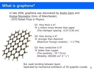
Graphing and Grafting Graphene: Classifying Finite Topological Defects (PRB 83, 195425 (2011); arXiv:1106.6273) Eric Cockayne, Joseph Stroscio, Gregory Rutter, Nathan Guisinger, Jason Crain NIST Phillip First Georgia Tech. Subject of the 2010 Nobel prize in Physics.

E N D
Graphing and Grafting Graphene: Classifying Finite Topological Defects (PRB 83, 195425 (2011); arXiv:1106.6273) Eric Cockayne, Joseph Stroscio, Gregory Rutter, Nathan Guisinger, Jason Crain NIST Phillip First Georgia Tech
Castro-Neto, Nature Mater. 6, 176 (2007). Castro-Neto et al., Physics World (2006) Graphene: Unusual electronic structure makes it a promising candidate for applications Microelectronics: high carrier mobility → high speed devices Resistance standard → unusual quantum Hall effect Commercial applications will require methods for large-scale production
Graphene production methods Mechanical exfoliation from graphite Chemical exfoliation from graphite Chemical reduction of graphene oxide Segregation of carbon from metal carbides Chemical vapor deposition of C onto metal surfaces Thermal desorption of Si from SiC Growth of graphene from by thermal desorption of Si from SiC very promising, but defects frequently observed Goal of this talk: elucidate nature of defects with the ultimate aim of (1) reducing or eliminating the defects or (2) generating defects at will to tune properties. Key results of this work: Topological defects are among the most common. Systematic way of describing and identifying topological defects found.
Topological defects in graphene: Changing the number of sides in a ring (replacing hexagons with pentagons, heptagons, etc. sp2 bonding: C planar; 3 neighbors Average number of sides = 6 exactly R. Phillips et al, PRB 46, 1941 (1992). Average < 6; positive curvature; buckyballs Average >6; negative curvature: “schwartize” Keep” flat”: defect with more than 6 membered ring must be compensated with ring with < 6 members & vice versa
Positive and negative disclinations: parents of all topological defects in graphene
Combine one positive and one negative disclination: obtain dislocation core.
Grain boundary that closes on itself: Grain boundary loop The grain boundary loop is the first type of topological defect shown in this talk that is “local” Local topological defect: core region of defect surrounded by lattice that is topologically equivalent to defect-free graphene Because only the core region is “disturbed”, these defects might be created or annihilated by the rearrangement of relatively few C atoms May be among most important defects in graphene Hypothesis: defects seen in earlier STM images are local topological defects. “Flower” defect
Computational Methods Ab initio electronic structure VASP used DFT, ultrasoft pseudopotentials 212 eV plane wave cutoff; Up to 864 atoms in supercell 8748 k points per BZ of primitive cell STM topographs simulations Tersoff approximation: Fixed V Current proportional to local density of states between Fermi level and bias V Tight binding model C 2pz levels put into model (Tanaka et. al., Carbon) Parameters determined via least squares fitting to ab initio data Up to 3888 atoms for bilayer supercell
Simulated STM images of the “flower” defect matches experiment. Cockayne et al., PRB 83, 195425 (2011).
Scanning tunneling spectroscopy of defects: energy-resolved information dI/dV plot ~ local density of states sharply peaked in energy, about 0.5 eV above the Dirac point
Experimental dI/dE plots compared w/ computed density of states Three computed peaks in experimental range. Why is only one seen?
Calculated DOS corresponding to each peak: The wavefunction of peak 1 is clearly different from the rest. Although peak 4 looks superficially similar to the resonance of peaks 2 and 3, tight binding calculations show that it has a different symmetry. Tight binding model confirms that peaks 2 and 3 come from single resonance inside flower region at ED + 0.3 eV and suggests that peak 4 is weak, explaining experimental observation of single peak
Energetic/Mechanical properties of flower defect: Lowest energy per 5-7 pair of any known topological defect Likely to coalesce mobile dislocation cores if they can not heal out. Also has large DA/DE: May increase strength of graphene under isotropic tension
Ideal graphene Cut Rotate “Flower” defect: Equivalent to rotating a portion of graphene with respect to the rest: Paste
A variety of rotational grain boundaries exist with different symmetries, number of core atoms rotated, and rotation angle
(2,1) (3,1) (4,1) Under hexagonal symmetry, there exists a whole family of rotational grain boundaries Labeled by pair of integers (m,n) Central 6 m2 atoms rotated by 60o (n/m) (4,2)
It is also possible to create a grain boundary loop by cutting out a region and then splicing a region with a different number of C atoms. As long as the number of “dangling bonds” is equal, the threefold bonding requirement will be satisfied. This allows for divacancies and di-interstitials to reconstruct and lower energy Need systematic way to classify “grain boundary loop” defects
Key to systematic classification: describe graphene defect structures in terms of the dual lattice. Dual lattice: n-vertices go to n-tiles and vice versa. Dual lattice of the graphene honeycomb structure is triangular. sp2 bonding (all vertices 3-vertices) means that all dual structures consist of triangles only
Work in “dual space” Don’t design defective graphene structures. Design defective triangle structures, and then take dual. In analogy with Stone-Wales defect, one can take any patch of triangles, and retriangulate in a way that preserves the perimeter. (examples will be shown in next slides). Structures will presumably have low energy if the retriangulation is also a patch of the ideal triangular lattice. Then, in terms of the graphene structure, one cuts out a patch and then “splices” or “transplants” a different patch of graphene with the same number of dangling bonds. Interesting mathematical result follows: topological defects that preserve sp2 bonding can only keep the number of atoms identical or change it by a multiple of 2.
Rule of thumb: topological defects in graphene prefer to have alternating 5-rings and 7-rings. Above image: graphene grain bounday (Huang et al., Nature (2011)).
One can design a defect with alternating 5-rings and 7-rings in dual space by choosing a replacement patch in dual space where the vertices have alternately +1 and -1 the number of triangles of the original. Metaphorically, one looks for “most compatible donors”
The complete set of “most-compatible donor” topological defects (with constraints on size and change in number of atoms <=2) is shown on right An infinite number of larger defects exists. The graphical representation of each defect is to draw an arrow connecting the original patch of triangles in the dual (opposite side) to the replacment patch (same side). The topological defects occur as inverse pairs. Shown are change in number of atoms (top) and DFT formation energy (in eV, bottom).
Simulated STM images of small topological defects. b a d c f e h g
J. Kotakoski et al., Phys. Rev. Lett. 106 105505 (2011) In addition to exploring defects systematically, the above paper suggests looking at defect clusters in addition to isolated local defects.
Previously unidentified experimental defects identified as isolated divacancies (top right) or divacancy clusters (double divacancy, bottom left)), (triple divacancy (bottom right)
The triple divacancy has a triangle of carbon atoms in the center!
Is this right? Triple divacancy Experiment Single vacancy
Conclusions • Dual space gives a graphical representation for finite topological defects in graphene • Low energy defects can be designed via “most compatible donor” procedure • Previously unidentified defects in graphene are identified as divacancies or divacany clusters • One such defect contains a planar triangle of carbons, an unusual structural motif
Other Graphene defects: Impurity atom Intercalation Substitution Substitution Adatom Defect atom can be anything: focus on Mo and Si Best fit: intercalated Mo Defect atom can be anything
Graphene layers remain nearly flat (h < 0.25 A) for intercalated Mo Magnetism? Mo position Magnetic moment M(B) isolated atom 6.0 adatom 0.0 intercalated 0.0 substitution 2.0 c/w M = 2.0 for Cr substitution in monolayer (Krasheninnikov et al., PRL 102, 126807 (2009); Santos et al,arXiv:0910.0400)
324 C + 1 Mo: DOS shows three defect-associated peaks near EDirac
Can individual state(s) be identified that match experimental STM images? Plots a-g show, in order of increasing energy, the zone center states near EDirac with significant Mo d participation State E-EDirac mult. a -0.57 2 b -0.49 1 c -0.17 2 d +0.02 2 e +0.20 1 f +0.33 2 g +0.88 2 Range of E ~ 1.5 eV Bright center: singlet; m = 0; dark center; doublet; m nonzero