Download

1 / 30
410 likes | 857 Views
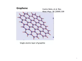
Graphene. Castro-Neto, et al. Rev. Mod. Phys. 81 (2009) 109. Single atomic layer of graphite. Graphene Electronic Properties (isolated graphene sheets) Graphene Formation—Growth on SiC Graphene Growth on BN, Co 3 O 4 , etc. Castro-Neto, et al. Rev. Mod. Phys. 81 (2009) 109.

E N D
Graphene Castro-Neto, et al. Rev. Mod. Phys. 81 (2009) 109 Single atomic layer of graphite
Graphene Electronic Properties (isolated graphene sheets) Graphene Formation—Growth on SiC Graphene Growth on BN, Co3O4, etc.
Graphene’s band structure yields unusual properties Castro Neto EF The velocity of an electron at the Fermi level (vF) Is inversely related to meff Effective mass (m*) ~ [dE2/dk2]-1 Most semiconductors, 0.1 m0 < m* < 1 me Graphene, m* < 0.01 m0 (depending on number of carriers) Therefore, expect VERY high mobility in graphene Both holes and electrons can be carriers
Castro-Neto, et al. Rev. Mod. Phys. 81 (2009) 109 Effective mass for graphene does get very small as n~ 1012
The Big Problem with graphene: an imagined conversation: A. OK: Graphene is great, lots of interesting properties for devices! B. How do you make a device? A. You need a sheet of graphene! B. OK, how do you get a sheet of graphene? A. HOPG, scotch tape, and tweezers! B. !@#$%%
How do you “grow” graphene? You can evaporate Si from SiC(0001) (either face) Popularized by the de Heer group at Georgia Tech.
Can grow multilayer films of graphene on SiC (azimuthally rotated from each other—electronically decoupled!) Anneal at 1350 C Interfacial layer (anneal at 1150 C) SiC Auger, graphene growth on SiC, deHeer et al.
Inverse photoemission and LEED (Forbeaux, et al, PRB, 58 (1998) 16396) Growth of graphite on SiC(0001) π* feature
Angle resolved UPS (Emtsev, et al, PRB 77(2008) 155303) shows transition to graphene band structure
Adjacent layers on graphene /SiC are decoupled from each other, Due to azimuthal rotation
Graphene on SiC(0001) Not uniform on an atomic level, different regions due to different #s of layers, orientations M B
Graphene/SiC photoemission: varying hv can vary the sampling depth (Emtsev, et al, PRB 77 (2008) 155303
The covalently bound stretched graphene (CSG model) Emtsev, et al., PRB 77 (2008) 155303
Pertinent Questions: How do Adjacent Graphene Sheets couple electronically? Single layer Graphene (good) Many layerGraphite (meh!?) Answer: On SiC, Adjacent Sheets apparently not coupled due to azimuthal rotation When/how this transition occurs is very pertinent to devices
Core (left) and valence band (right) PES graphene growth on SiC (Emtsev, et al) Explain the implications of this for graphene coupling between layers
Motivation: Direct Growth on Dielectric Substrates: Toward Industrially Practical, Scalable Graphene—Based Devices Graphene Growth: Conventional Approaches transfer CVD graphene monolayer Result: graphene SiO monolayer, interfacial inhomogeneities 2 Co3O4(111) Metal or HOPG Si graphene Si evaporation Result: graphene > 1500 K monolayer or multilayer SiC (0001) SiC (0001) on SiC (0001) Co(111) or Si(100)-gate FET: Band gap Our Focus: Direct CVD, PVD or MBE On Dielectrics Charge-based devices Top Gate n graphene Spintronics MgO(111) Si(100) Coherent-Spin FET: Multi-functional, non-volatile devices
Hemispherical analyzer (XPS) ALD or PVD Free radical source LEED Sample Intro chamber P = 103 Torr – 10-6 Torr Sample processing P = 10-9 -10-3 Torr UHV Analysis Chamber P ~ 5 x 10⁻¹⁰ Torr Butterfly valve Gate NH3 BCl3 Graphene/Co3O4 valves Turbo Graphene/MgO(111) Intro/ deposition transfer MBE Sample heating to 1000 K @ 1 Torr STM Auger UHV chamber, 10-11 Torr Graphene growth & characterization without ambient exposure LEED I(V)
Graphene/BN/Ru(0001): Bjelkevig, et al LEED shows BN and Graphene NOT azimuthally rotated! Orbital hybridization with Ru 3d!
Gr/BN/Ru(0001): Inverse photoemission. π* not observed! BN layer does NOT screen graphene from orbital hybridization and charge transfer from Ru!
Graphene on Co3O4(111): Molecular Beam Epitaxy Substrate Preparation Evaporator P~ 10-8 Torr 750 K Co(111)+ dissolved O Sapphire(0001) Sapphire(0001) Sapphire(0001) 1000 K/UHV ~3 ML Co3O4(111) Co(111) O segregation
Graphene growth on Co3O4(111)/Co(0001) MBE (graphite source)@1000 K: Layer-by-layer growth 1st ML 3 ML 2nd ML 0.4 ML M. Zhou, et al., J. Phys.: Cond. Matt. 24 (2012) 072201
LEED: Oxide/Carbon Interface is incommensurate: Different than graphene on SiC or BN! Graphene Domain Sized (from FWHM) ~1800 Å (comp. to HOPG) 65eV (a) (b) graphene 0.4 ML Co3O4(111) 65 eV beam energy (d) (c) 3 ML 65eV Oxide spots attenuated with increasing Carbon coverage 2.5 Å 2.8 Å M. Zhou, et al., J. Phys.: Cond. Matt. 24 (2012) 072201 2.8 Å O-O surface repeat distance on Co3O4(111) W. Meyer, et al. JPCM 20 (2008) 265011
XPS: C(1s) Shows π system: Binding Energy indicates graphene oxide charge transfer XPS (separate chamber): Al Kα source 284.9(±0.1) eV binding energy: Interfacial polarization/charge transfer to oxide No C-O bond formation π→π* M. Zhou, et al., J. Phys.: Cond. Matt. 24 (2012) 072201
Directly grown graphene/metals and dielectrics: Inverse photoemission and charge transfer Position of * (relative to EF) indicates direction of interfacial charge transfer (Kong, et al., J.Phys. Chem. C. 114 (2010) 21618 n-type charge transfer p-type Ef Forbeaux, et al. Multilayers
Generalization, Directly Grown Graphene and Charge Transfer: Oxides (p-type) vs. Metals (n-type) graphene graphene EF e- n-type; metal to graphene charge transfer Transition metals (Ru, Ni, Cu, Ir…) p-type; graphene to substrate charge transfer e- Oxides, SiC EF
Suspended graphene • Graphene (few layer) on Co3O4: • Much more conductive than suspeneded graphene • Why?? • Significant doping????? • High mobility (How high)?????
Conclusion: Graphene: Large area growth on practical substrates critical for device development. Interactions with substrates and (maybe) other graphene layers are critical to device properties