Download
1 / 2
20 likes | 109 Views
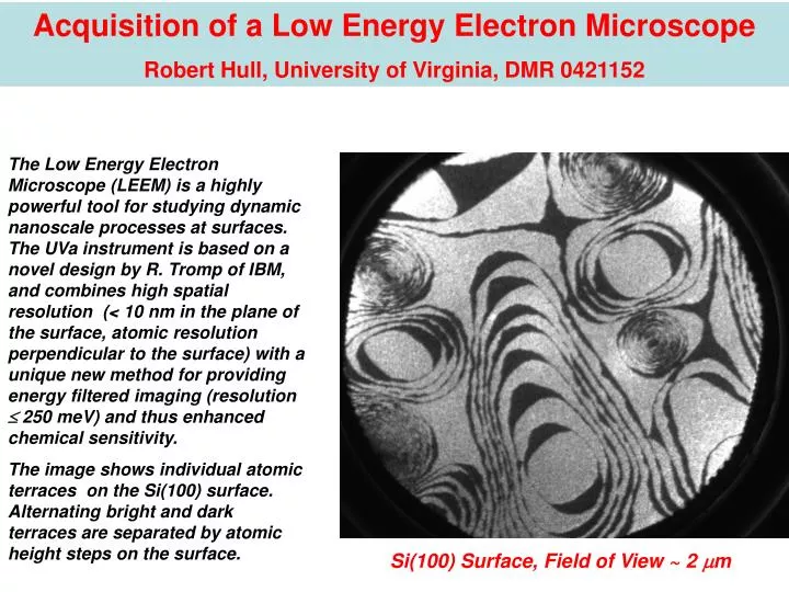
Acquisition of a Low Energy Electron Microscope Robert Hull, University of Virginia, DMR 0421152.

E N D
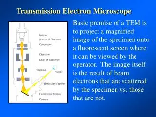
Acquisition of a Low Energy Electron Microscope Robert Hull, University of Virginia, DMR 0421152 The Low Energy Electron Microscope (LEEM) is a highly powerful tool for studying dynamic nanoscale processes at surfaces. The UVa instrument is based on a novel design by R. Tromp of IBM, and combines high spatial resolution (< 10 nm in the plane of the surface, atomic resolution perpendicular to the surface) with a unique new method for providing energy filtered imaging (resolution 250 meV) and thus enhanced chemical sensitivity. The image shows individual atomic terraces on the Si(100) surface. Alternating bright and dark terraces are separated by atomic height steps on the surface. Si(100) Surface, Field of View ~ 2 m
Robert Hull, University of Virginia, DMR 0421152 • Additional Notes • The image is formed using an aperture around one of the superstructure reflections from the (2x1) reconstructed surface. Terraces diffracting into this reflection appear bright, while those with the orthogonal surface dimerization direction diffract into the orthogonal reflection in the diffraction pattern and thus appear dark. The boundaries between bright and dark regions correspond to monolayer steps on the surface. Note that fields of view are not yet accurately calibrated, hence the “~” symbol before the “2 um” in the figure caption. • Imaging the Si(100) surface by LEEM is not new, but obtaining images of this quality is a crucial step in ensuring the UVa instrument is operating at full performance • The energy filtered imaging capability is an entirely new design by Ruud Tromp, employing scanning slits in entrance and exit diffraction planes of the magnetic prism. It has already demonstrated 250 meV resolution (after deconvoluting energy spread from the electron source). • UVa student Jacob Thorp worked in Tromp’s lab at IBM for several weeks this summer. • We have separate funding from the Semiconductor research Corporation (with Tromp and with Peter Sutter at Brookhaven National Lab) to explore improvements in spatial, temporal and energy resolution.