Download
1 / 9
190 likes | 714 Views
GaAs MESFET Process Flow. Wafer Cleaning Device Processing. Wafer Cleaning. Degreasing (grease) Boil the substrate in Trichloroethane (TCE – 80 C) for 10 minutes (hard grease) Soak in warm Acetone (50 C) for 10 minutes (light grease and polymers) Soak in IPA (2-propanol) for 10 minutes

E N D
GaAs MESFET Process Flow Wafer Cleaning Device Processing
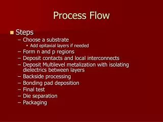
Wafer Cleaning • Degreasing (grease) • Boil the substrate in Trichloroethane (TCE – 80 C) for 10 minutes (hard grease) • Soak in warm Acetone (50 C) for 10 minutes (light grease and polymers) • Soak in IPA (2-propanol) for 10 minutes • Flush with cold IPA • Blow dry with N2 • RCA cleaning (oxides, metal contaminants) • Immerse GaAs in 1:1 solution of HCL:DI-water for 5 minutes • Immerse GaAs in 1:1 solution of NH4OH:DI-water for 5 minutes • Immerse GaAs in DI-water for 5 minutes • Blow dry with N2
Photoresist (positive) GaAs MESFET Process Flow • Start with a n-GaAs / SI-GaAs wafer • Apply positive-Photoresist (S-1813) n-GaAs SI-GaAs
GaAs MESFET Process Flow • Apply 1st mask to form the S/D ohmic contact pattern • Apply UV-light • Exposed PR will become softer • Develop (MF-319 - 45 sec.) the photoresist and remove soft parts hard PR soft PR n-GaAs SI-GaAs
GaAs MESFET Process Flow • S/D ohmic contact deposition (AuGeNi) – deposit them first and then thermal annealing – thicknesses ??? • Lift-off (with acetone and ultrosonic agitation) AuGeNi • Apply PR to form the gate • Apply the mask and expose the wafer to UV light hard PR n-GaAs SI-GaAs
GaAs MESFET Process Flow • Develop the photoresist • Evaporate TiPtAu AuGeNi • Lift off TiPtAu n-GaAs SI-GaAs
GaAs MESFET Process Flow • First metallization AuGeNi • Develop the PR TiPtAu • Evaporate TiAu • Lift-off TiAu n-GaAs SI-GaAs
GaAs MESFET Process Flow AuGeNi • Silicon-Nitride for electrical isolation TiPtAu TiAu n-GaAs SI-GaAs
Final Device AuGeNi * Optical lithography, feat.res. ~ 0.5-1 µm TiPtAu * Ti( 250 A) / Au (1500 A) TiAu Source Drain Gate 2.5µm TiAu ~ 2.5µm TiPtAu AuGeNi n-GaAs 1.5 µm SI-GaAs 1-2 µm