Download
1 / 31
330 likes | 679 Views
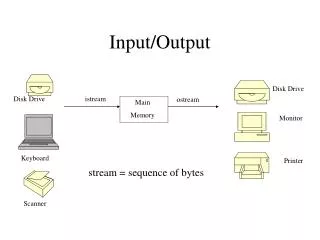
Input / Output (Peripheral) Interfacing. Peripheral devices. Peripheral devices Input devices such as keyboard, switches, Mouse, Microphone Output devices such as LED, LCD, Monitor, Printer, Speaker. Peripheral devices vs. Memory.

E N D
Peripheral devices • Peripheral devices • Input devices such as keyboard, switches, Mouse, Microphone • Output devices such as LED, LCD, Monitor, Printer, Speaker
Peripheral devices vs. Memory • like a memory chip, it is mapped to a certain location (called the port address) • unlike a memory chip, a peripheral is usually mapped to a single location
Peripheral devices vs. Memory (continue) • like a memory chip, you can write to an output device • You can write to a memory chip using the command such as mov [2000], al • You can write to an output device using the OUT command
Peripheral devices vs. Memory (continue) • like a memory chip, you can read from an input device • You can read from a memory chip using the command such as mov al, [4000] • You can read from an input device using the IN command
Format 1: 8 bit address IN AL, port# example: IN AL, 40H Or OUT port#, AL example: OUT E3H, AL Can address up to 256 I/O devices Two formats for IN / OUT Instruction I/O MAP 00 H 01 H FF H
Format 2: 16 bit address MOV DX, port#IN AL, DX Example: MOV DX, 2500H IN AL, DX Or MOV DX, port#OUT DX, AL Example: MOV DX, FF00H OUT DX, AL Can address up to 64k I/O devices Two formats for IN / OUT Instruction I/O MAP 0000 H 0001 H FFFF H
Processor Timing Diagram for any I/O write (OUT instruction) machine cycle
Creating a Simple Output Device(16 bit address format) • Use 8-LED’s as output device • Assign an address for this output device for example F000H • Use a Latch and an address decoder such that the LED’s will only respond to the command out with a specific address (let’s assume that the address is F000) and latch the data
D0 Q0 D1 Q1 D2 Q2 D3 Q3 D4 Q4 74LS373 D5 Q5 D6 Q6 D7 Q7 LE OE Use of 74LS373 and Address Decoder A19 A18 : A0 : mov al, 55 mov dx, F000 out dx, al : D7 D6 D5 D4 D3 D2 8088 D1 Minimum D0 Mode IOR IOW Address Decoder A A A A A A A A A A A A A A A A IOW 1 1 1 1 1 1 9 8 7 6 5 4 3 2 1 0 5 4 3 2 1 0
Processor Timing Diagram for any I/O read (IN instruction) machine cycle
Creating a Simple Input Device • Use 8-Switches (keys) • Assign an address for this input device for example F000H • Use 8 bit tri state gate (74244) and an address decoder such that the keys will be read only with the command IN at a specific address (let’s assume that the address is F000)
A0 B0 A1 B1 A2 B2 A3 B3 A4 B4 74LS244 A5 B5 A6 B6 A7 B7 E Use of 74LS245 and Address Decoder 5V A19 A18 : A0 D7 : mov dx, F000 in al, dx : D6 D5 D4 D3 D2 8088 D1 Minimum D0 Mode IOR IOW Address Decoder Same address for input and output? A A A A A A A A A A A A A A A A IOR 1 1 1 1 1 1 9 8 7 6 5 4 3 2 1 0 5 4 3 2 1 0
Output Port Design (8 bit address format) We assign output port address as 99H ( 1001 1001 B )
Input Port Design (8 bit address format) We assign input port address as 5FH ( 0101 1111B )
تمرین: (چراغ راهنمایی) سه LED سبز، قرمز و زرد از طریق یک لچ 74373 به cpu اینترفیس شده است برنامه ای به زبان اسمبلی 8088 بنویسید که به ترتیب LED سبز 70 ثانیه LED زرد 4 ثانیه و LED قرمز 50 ثانیه روش شده و این کار تکرار شود. فرکانس کلاک اعمالی به CPU را 8MHZ در نظر بگیرید. آدرس پرت خروجی را 5EH فرض نمایید.
8255 Features • One of the most widely used I/O chips • Is a 40-pin DIP chip • Has three separately accessible ports, A, B, and C • which can be programmed as input or output • Has the capabilities of 74373 and 74244 together
8255 Pin description • Port A (PA0-PA7): This 8-bit port A can be programmed all as • input or all as output • PB(PB0-PB7): This 8-bit port B can be programmed all as • input or all as output • PC(PC0-PC7): This 8-bit port C can be all input or all output. • It can also be split into two parts, CU (upper bits PC4-PC7) • and CL (lower bits PC0-PC3). Each can be used for input or • output. Any of PC0 to PC7 can be programmed individually. • RD’ and WR’: (inputs) IOR and IOW of the system bus are • connected to these two pins.
8255 Pin description (cont.) • RESET:(input) used to clear control register. When RESET • is activated, all ports are initialized as input ports. This pin must be connected to the RESET output of the system bus. • A0, A1 and CS’(chip select): While CS selects the entire chip, address pins A0 and A1 select the specific port within the 8255. These three pins are used to access ports A, B, C, and the control register, as shown in Table 11-3. • D0-D7: Data bus of chip which are connected to CPU data bus.
Mode selection of the 8255 • While ports A, B and C are used for I/O data, it is the control register that must be programmed to select the operation mode of the three ports A, B and C.
The modes of 8255 ports • Mode 0, simple I/O mode. In this mode, any of the ports A, B, CL and CU can be programmed as input or output. In this mode, all bits are out or all are in. In other words, there is no control of individual bits. • Mode 1. In this mode, ports A and B can be used as input or output ports with handshaking capabilities. • Mode 2. In this mode, port A can be used as a bidirectional I/O port with handshaking capabilities.
Programming of 8255 • The 8255 is programmed in any of the mode by sending a byte (Intel calls it control word) to the control register of the 8255 (as shown in fig. 11-12)
BSR(Bit Set Rest) mode • In BSR mode, we can set or reset bits of port C individually • We can do it by writing a proper control word in control register (as shown in fig 5 )
Example for BSR • Program 8255 for the following • A) set PC2 to high • B) Use PC6 to generate a square wave of 66% duty cycle • Solution • A) • MOV AL, 00000101BOUT 93H,AL • B) • AGAIN MOV AL, 0xxx1101 OUT 93H, AL CALL Delay CALL Delay MOV AL, 0xxx1100 OUT 93H, AL CALL Delay JMP AGAIN