Download
1 / 10
110 likes | 267 Views
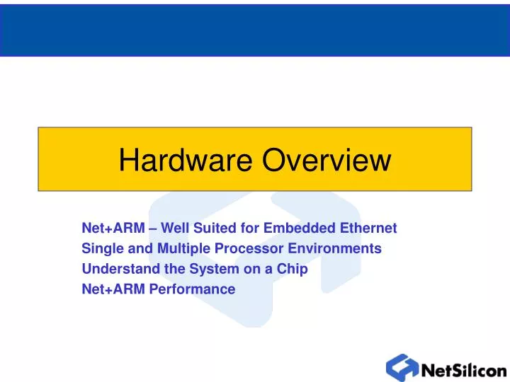
Hardware Overview. Net+ARM – Well Suited for Embedded Ethernet Single and Multiple Processor Environments Understand the System on a Chip Net+ARM Performance. Network. Why the NET+ARM is Well Suited for Embedded Ethernet Projects …. ARM7 CPU. Cache RAM. Cache Utilization. Cache Control.

E N D
Hardware Overview Net+ARM – Well Suited for Embedded Ethernet Single and Multiple Processor Environments Understand the System on a Chip Net+ARM Performance
Network Why the NET+ARM is Well Suited for Embedded Ethernet Projects … ARM7 CPU Cache RAM Cache Utilization Cache Control Ethernet Serial ENI 1284 GPIO MEM &BUS DMA External RAM
Network NET+ARM™ System OverviewSingle Processor Environment Reset Power FLASH • SDRAM • EDO DRAM • FP DRAM • SRAM Clock JTAG RAM Optional Co-Processor Interface Shared RAM FIFO Additional I/O Three Additional Chip SelectsAvailable for External Hardware 8, 16, or 32 Bit PeripheralsIndependently ConfiguredExternal Bus Master Capable ENI Interface UART, HDLC, SPI Supported… Serial Port Line Driver JTAG RS232, 422, 485DMA Support Serial Port Line Driver DMA CAPABLE Physical Layer Transformer RJ45 Serial Interface DMA Support
JTAG Network NET+ARM™ System OverviewMultiple Processor Environment Data movement to / from external processor Reset Power FLASH • SDRAM • EDO DRAM • FP DRAM • SRAM RAM External Processor ENI Three Additional Chip SelectsAvailable for External Hardware 8, 16, or 32 Bit PeripheralsIndependently ConfiguredExternal Bus Master Capable FLASH RAM JTAG • Shared RAM • Up to 64K of NET+ARM RAM designated • FIFO • Two 32 Byte FIFOs supported by DMA • NET+ARM ENI INTERFACE is a SLAVE DMA CAPABLE Serial Interface Physical Layer Transformer RJ45 DMA Support
Interrupt DMA Timer GPIO Ethernet Controller Bus Arbiter Bus Controller Memory Controller Clock Understanding the SoC Peripherals GEN Module ENI ARM7 Core Cache Serial Controller Peripherals
TYPICAL DESIGN NET+ARM™ Performance(X32 SDRAM with Multiple DMA Channels) BUS MASTERING EACH BUS MASTER IN THE CURRENT CYCLE CAN MOVE 4 LONG WORDS… MUST THEN GIVE UP THE BUS IF ANOTHER BUS MASTER IS WAITING 11 11 11 ENI External ARM7 DMA POTENTIAL BUS MASTERS 4-1-1-1 4-1-1-1 NOTE 1 DMA1 ARM7 DMA1 ARM7 ARM7 DMA2 ARM7 DMA2 78 Mbytes / Sec 78 Mbytes / Sec 78 Mbytes / Sec 78 Mbytes / Sec 78 Mbytes / Sec 78 Mbytes / Sec 78 Mbytes / Sec 78 Mbytes / Sec WITH NO CACHE SAME CYCLE WITH CACHE DMA1 ARM7 DMA1 DMA1 ARM7 DMA1 ARM7 78 Mbytes / Sec 78 Mbytes / Sec 78 Mbytes / Sec 78 Mbytes / Sec 78 Mbytes / Sec OVER 2 CYCLES EQUATES TO … 78 Mbytes / Sec on DMA 78 Mbytes / Sec with ARM OVER 2 CYCLES EQUATES TO … 39 Mbytes / Sec 8.5 MIPS 78 Mbytes/Sec 40 MIPS • Assuming SDRAM @ 4-1-1-1 Burst • CACHE is Single Cycle Memory • Frequency 44.236MHz NOTE 1: DMA Context Switch Time 13 BCLKS
TYPICAL DESIGN ARM7 DMA1 ARM7 DMA1 DMA1 DMA1 ARM7 DMA1 78 Mbytes / Sec 78 Mbytes / Sec 78 Mbytes / Sec 78 Mbytes / Sec 78 Mbytes / Sec 78 Mbytes / Sec 78 Mbytes / Sec 78 Mbytes / Sec WITH NO CACHE SAME CYCLE WITH CACHE ARM7 DMA1 ARM7 ARM7 DMA1 ARM7 DMA1 78 Mbytes / Sec 78 Mbytes / Sec 78 Mbytes / Sec 78 Mbytes / Sec 78 Mbytes / Sec OVER 2 CYCLES EQUATES TO … 78 Mbytes / Sec on DMA 78 Mbytes / Sec with ARM OVER 2 CYCLES EQUATES TO … 8.8 MIPS 39 Mbytes / Sec 78 Mbytes/Sec 40 MIPS NET+ARM™ Performance (X32 SDRAM with 1 DMA Channel) BUS MASTERING EACH BUS MASTER IN THE CURRENT CYCLE CAN MOVE 4 LONG WORDS… MUST THEN GIVE UP THE BUS IF ANOTHER BUS MASTER IS WAITING ENI External ARM7 DMA POTENTIAL BUS MASTERS 4-1-1-1 11 4-1-1-1 11 11 • Assuming SDRAM @ 4-1-1-1 Burst • CACHE is Single Cycle Memory • Frequency 44.236MHz
ARM7 DMA ARM7 DMA DMA DMA ARM7 DMA 106 Mbytes / Sec 106 Mbytes / Sec 106 Mbytes / Sec 106 Mbytes / Sec 106 Mbytes / Sec 106 Mbytes / Sec 106 Mbytes / Sec 106 Mbytes / Sec WITH NO CACHE SAME CYCLE WITH CACHE ARM7 DMA ARM7 ARM7 DMA ARM7 DMA 106 Mbytes / Sec 106 Mbytes / Sec 106 Mbytes / Sec 106 Mbytes / Sec 106 Mbytes / Sec OVER 2 CYCLES EQUATES TO … 106 Mbytes / Sec on DMA 106 Mbytes / Sec with ARM OVER 2 CYCLES EQUATES TO … 12 MIPS 53 Mbytes / Sec 106 Mbytes/Sec 40 MIPS NET+ARM™ Performance (X32 SRAM with 1 DMA Channel) TYPICAL DESIGN EACH BUS MASTER IN THE CURRENT CYCLE CAN MOVE 4 LONG WORDS… MUST THEN GIVE UP THE BUS IF ANOTHER BUS MASTER IS WAITING ENI External ARM7 DMA POTENTIAL BUS MASTERS 2-1-1-1 2-1-1-1 • Assuming SRAM @ 2-1-1-1 Burst • CACHE is Single Cycle Memory • Frequency 44.236MHz
DMA1 ARM7 DMA1 ARM7 ARM7 ARM7 DMA2 ARM7 106 Mbytes / Sec 106 Mbytes / Sec 106 Mbytes / Sec 106 Mbytes / Sec 106 Mbytes / Sec 106 Mbytes / Sec 106 Mbytes / Sec 106 Mbytes / Sec WITH NO CACHE SAME CYCLE WITH CACHE DMA1 ARM7 DMA1 DMA1 ARM DMA1 ARM7 106 Mbytes / Sec 106 Mbytes / Sec 106 Mbytes / Sec 106 Mbytes / Sec 106 Mbytes / Sec OVER 2 CYCLES EQUATES TO … 106 Mbytes / Sec on DMA 106 Mbytes / Sec with ARM OVER 2 CYCLES EQUATES TO … 8.5 MIPS 38 Mbytes / Sec 106 Mbytes/Sec 40 MIPS NET+ARM™ Performance (X32 SRAM with Multiple DMA Channels) TYPICAL DESIGN EACH BUS MASTER IN THE CURRENT CYCLE CAN MOVE 4 LONG WORDS… MUST THEN GIVE UP THE BUS IF ANOTHER BUS MASTER IS WAITING ENI External ARM7 DMA POTENTIAL BUS MASTERS 2-1-1-1 2-1-1-1 NOTE 1 • Assuming SRAM @ 2-1-1-1 Burst • CACHE is Single Cycle Memory • Frequency 44.236MHz NOTE 1: DMA Context Switch Time 13 BCLKS
Hardware Overview Summary • Up to four bus masters: ARM7, DMA, ENI, External • Bus master must relinquish the bus to another waiting master after four long words transferred • Cache permits ARM7 to move data concurrently with DMA • DMA cannot operate on cached memory • DMA channel context switch requires 13 clock cycles