Download

1 / 18
190 likes | 341 Views
Microfluidic Impedance Spectroscopy System. First Design Review. Matthieu Giraud-Carrier Kyra Moon 02/08/2011. Overview. Introduction Purpose Motivation Product Design Project Requirements Design Specifications Customer Needs Alternate Concepts Concept Selection and Generation

E N D
Microfluidic Impedance Spectroscopy System First Design Review Matthieu Giraud-Carrier Kyra Moon 02/08/2011
Overview • Introduction • Purpose • Motivation • Product Design • Project Requirements • Design Specifications • Customer Needs • Alternate Concepts • Concept Selection and Generation • Fundamental Design Issues • Critical Concepts • Schedule • Current and Future Work
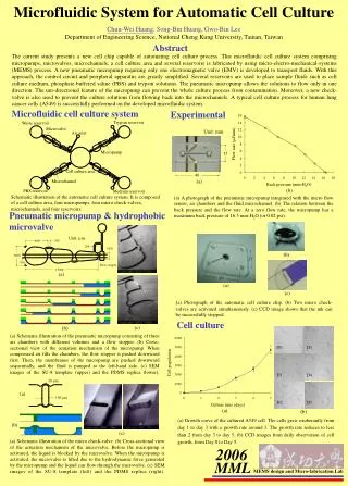
Introduction—Purpose • Basic goal: Build a microfluidic impedance spectroscopy system. • In other words -- build a chip with a small channel which can be filled with fluids (primarily protein solutions) and then analyzed.
Introduction—Motivation • Medical field – researchers can learn how these proteins interact by observing the electrical properties of these solutions over a wide frequency range. • Creating microfluidic systems out of inexpensive materials would facilitate medical research by making it less expensive and easier to use.
Introduction—Product Design • The final product: A chip of a few square inches. • Basic elements: • Waveguide runs through the chip and is terminated by an SMA connector on either side. • Microfluidic channel close to the waveguide (three copper lines) in the center of the chip. • Reservoir that ensures the channel will always be full during analysis. The user will also be able to connect to these reservoirs through a standard pressurized port.
Design Specifications • Bandwidth: 100MHz to 7GHz • Volume of channel: 0.5mm X 1mm X 2cm (10uL) • Accuracy (% repeatability): 5% • Temperature stability: Within 1 degree • Final outputs: Conductivity and Permittivity (from S-Parameters) • Develop a numerical model for the waveguide (Sensitivity measures for changes in permittivity and conductivity) • Interface between Network Analyzer and Plotting Mechanism (GPIB, LabView, Matlab) • Materials: Standard PCB materials (FR-4, FR-2) • Sufficient reservoir volume for a 5-minute test • Connectors: SMA on board
Block Diagram • A user selects the liquid to be analyzed • Liquid is sent into the microfluidic channel through Nanoport connectors. • The Network Analyzer gathers information from the chip (using standard SMA connectors) • An interface turns the raw data from the analyzer into useful information for the user.
Alternate Concepts • Using acrylic instead of PCB material. • Using a waveguide perpendicular to the microfluidic channel rather than parallel. • Using a multilayer board to build the waveguide without direct contact to the channel. • Modifying the geometry of the channel and reservoirs and having the waveguide go straight across the chip • Making the waveguide run over the top of the channel on the main copper layer. • Using vias to avoid the 90 degree angle turns in the copper lines. • Using Prepreg to ensure no leakage.
Fundamental Design Issues • Material Selection: Decide what PCB type material will be optimal for our system. • Leakage Prevention: Design the board so that the protein solution can be confined properly to the channel. • Signal Path Geometry: Consider how to align the channel and waveguide and how to fit all the connections on the board.
Schedule – Critical Path • Determine how to set milling depth on machine • Learn how to create vias and alignment holes • Make several prototypes • Have board made professionally
Schedule – Categories • First category: learning how to use the devices and software. • Kyra – HFSS (modeling software), interfaces computer • Matthieu – milling machine, CAD software , how to create the boards • Second category: physically creating the board • It takes time to bond the board, run leakage tests, and create several prototypes • Third category: waiting for outside sources • Arrival of parts, making the chip professionally • We have little control over this category so we need to order early
Current & Future Work • Kyra is fine-tuning the current HFSS model. • We will soon be getting the Prepreg and running several tests to optimize bonding. • Still learning how to use the camera system on the milling machine. • Using Network Analyzer to run preliminary tests and gain intuition. By next design review: • All fabrication issues finalized and optimized. • Have a complete working model of our system in HFSS.