Download
1 / 16
160 likes | 338 Views
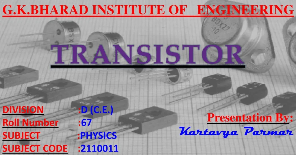
G.K.BHARAD INSTITUTE OF ENGINEERING. T RANSISTOR. DIVISION : D (C.E.) Roll Number : 67 SUBJECT : PHYSICS SUBJECT CODE : 2110011. Presentation By : Kartavya Parmar. About Transistor.

E N D
G.K.BHARAD INSTITUTE OF ENGINEERING TRANSISTOR DIVISION:D (C.E.) Roll Number:67 SUBJECT:PHYSICS SUBJECT CODE:2110011 Presentation By: Kartavya Parmar
The transistor, invented by three scientists at the Bell Laboratories in 1947, rapidly replaced the vacuum tube as an electronic signal regulator. • A transistor regulates current or voltage flow and acts as a switch or gate for electronic signals. A transistor consists of three layers of a semiconductor material, each capable of carrying a current. • A semiconductor is a material such as germanium and silicon that conducts electricity in a "semi-enthusiastic" way. It's somewhere between a real conductor such as copper and an insulator.
The semiconductor material is given special properties by a chemical process called doping. • The doping results in a material that either adds extra electrons to the material which is then called N-type for the extra negative charge carriers or creates "holes" in the material's crystal structure which is then called P-type because it results in more positive charge carriers. • The transistor's three-layer structure contains an N-type semiconductor layer sandwiched between P-type layers a PNP configuration or a P-type layer between N-type layers an NPN configuration.
A small change in the current or voltage at the inner semiconductor layer which acts as the control electrode produces a large, rapid change in the current passing through the entire component. The component can thus act as a switch, opening and closing an electronic gate many times per second. • Today's computers use circuitry made with complementary metal oxide semiconductor (CMOS) technology. CMOS uses two complementary transistors per gate. When one transistor is maintaining a logic state, it requires almost no power. • Transistors are the basic elements in integrated circuits (ICs), which consist of very large numbers of transistors interconnected with circuitry and baked into a single silicon microchip or "chip."
The transistor is an arrangement of semiconductor materials that share common physical boundaries. Materials most commonly used are silicon, gallium-arsenide, and germanium, into which impurities have been introduced by a process called "doping.“ • In n -type semiconductors the impurities or do pants result in an excess of electrons, or negative charges; in p -type semiconductors the do pants lead to a deficiency of electrons and therefore an excess of positive charge carriers or "holes."
The Junction Transistor • The n-p-n junction transistor consists of two n -type semiconductors separated by a thin layer of p -type semiconductor. The transistor action is such that if the electric potentials on the segments are properly determined, a small current between the base and emitter connections results in a large current between the emitter and collector connections, thus producing current amplification. • Some circuits are designed to use the transistor as a switching device; current in the base-emitter junction creates a low-resistance path between the collector and emitter. The p-n-p junction transistor, consisting of a thin layer of n -type semiconductor lying between two p -type semiconductors, works in the same manner, except that all polarities are reversed.
The Field-Effect Transistor • A very important type of transistor developed after the junction transistor is the field-effect transistor (FET). It draws virtually no power from an input signal, overcoming a major disadvantage of the junction transistor. An n -channel FET consists of a bar (channel) of n -type semiconductor material that passes between and makes contact with two small regions of p -type material near its center. The terminals attached to the ends of the channel are called the source and the drain; those attached to the two p -type regions are called gates. • A voltage applied to the gates is directed so that no current exists across the junctions between the p - and n -type materials; for this reason it is called a reverse voltage. Variations of the magnitude of the reverse voltage cause variations in the resistance of the channel, enabling the reverse voltage to control the current in the channel. A p -channel device works the same way but with all polarities reversed. The metal-oxide semiconductor field-effect transistor (MOSFET) is a variant in which a single gate is separated from the channel by a layer of metal oxide, which acts as an insulator, or dielectric. The electric field of the gate extends through the dielectric and controls the resistance of the channel. In this device the input signal, which is applied to the gate, can increase the current through the channel as well as decrease it.
Advantages of Transistor • Immediate functioning, no time for heating necessary. • Minimal losses and hardly any development of heat. • Smaller measurements and low weight. • Smaller mechanical sensitivity. • Fast switching. • Lower supply voltage. • Low susceptibility to trouble and long lifetime.
Disadvantages of Transistor • When they blow, they need to be replaced BUT they are so small (that an advantage) it can be difficult to find the offending transistor. • Manufacturing techniques are complex. • Manufacturing techniques require clean rooms. • They can be put into the circuit board the wrong way and therefore not work. • Removing them from a circuit board involves unsoldering whereas valves were plugged. • If they are on an integrated circuit and blow, the ENTIRE integrated circuit must be replaced.
Transistor as an Amplifier • A transistor can be used to amplify current. This is because a small change in base current causes a large change in collector current. • Example is a microphone. • Sound waves that are fed into the microphone cause the diaphragm in the microphone to vibrate. • The electrical output of the microphone changes according to the sound waves. • As a result, the base current is varying because of the small alternating voltage produced by the microphone. • A small change in the base current causes a large change in the collector current. • The varying collector current flows into the loudspeaker. There, it is changed into the sound waves corresponding to the original sound waves. • The frequencies of both waves are equivalent but the amplitude of the sound wave from the loudspeaker is higher than the sound waves fed into the microphone.
Transistor as Switch • In a transistor, no current can flow in the collector circuit unless a current flows in the base circuit. This property allows a transistor to be used as switch. • The transistor can be turned on or off by changing the base. • There are a few types of switching circuits operated by transistors. • Light-Operated Switch. • Heat-Operated Switch.