Download
1 / 31
310 likes | 415 Views
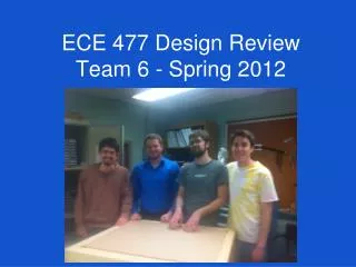
ECE 477 Design Review Team 2 Spring 2010 Digi -Brush. Josh Long . Katie Schremser. Caleb Ayew-ew. Outline. Project overview Project-specific success criteria Block diagram Component selection rationale Packaging design Schematic and theory of operation PCB layout

E N D
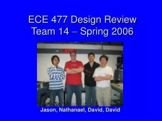
ECE 477 Design ReviewTeam 2 Spring 2010Digi-Brush Josh Long Katie Schremser Caleb Ayew-ew
Outline • Project overview • Project-specific success criteria • Block diagram • Component selection rationale • Packaging design • Schematic and theory of operation • PCB layout • Software design/development status • Project completion timeline • Questions / discussion
Project Overview • Child’s toy that can eliminate the mess and stress of children painting. • User can use multiple colors by mixing 8 given colors • Current color will be indicated through an LED in the tip of the brush • Painting will be recognized by interaction with a 15” touch screen • Image on the display can be saved onto an SD Card
Project-Specific Success Criteria • An ability to display images on the display board • An ability to track the digital brush on the display board • An ability to mimic paintbrush stroke characteristics on the display board • An ability to save the painted image on a SD card • An ability to distinguish user’s color selection and display selected color before being painted
Microcontroller :Freescale 9S12DP512DGV1 • 16-bit CPU (HCS12) • 512 kB Flash EEPROM (Program Memory) • Multiple Peripherals • 3 SPI (FPGA) • 2 8-channel, 10-bit ATD (Color pots, Touch Screen, Force Resistor) • 1 IIC (LED Driver) • Max Frequency of 50 MHz (with external oscillator) • 5V Operation
FPGA: Cyclone II EP2C20Q240C8 K ABB9Y0737A • 4 PLLs • 239,616 total RAM bits • 26 Embedded Multipliers • 3.3V , Max 260 MHz Operation • Easily Accessible VHDL Libraries • Low Cost
15” Touch Monitor/Touch Screen • 15” Size • Comparable to an 8.5” x 11” piece of paper • Cheaper than 12.1” for both parts combined • 15” Touch Monitor • Separate Monitor and Touch Screen were cheaper than a pre-packaged touch screen • 15” 5-Wire Resistive Touch Screen • Resistive technology allows recognition by items other than fingers • 5-Wire allows more accuracy than 4-Wire
Packaging Design 8 Color pots 1 “Water” Pot Brush Holder/Connector Save/Clear Buttons 15” LCD Monitor 15” Touch Screen
Theory of Operation • Power • Microcontroller • LED Driver • Color Pots • Force Resistor • Touch Panel • FPGA • Boot Chip • SDRAM • VDAC/Monitor • SD Card Reader
Theory of Operation: Power • 31V @ 2.4A inputs to linear regulators from a wall-wart • Three LM350 Linear Regulators • >=28V to: • 1.25V • 3.3V • 5V
Theory of Operation: Microcontroller • 50 MHz External Oscillator • 2 GPIO for Save and Clear Screen Pushbuttons • 5V Vdd
Theory of Operation: FPGA • 50 MHz External Oscillator • 133 MHz External Oscillator • 1.25V Internal • 3.3V Vdd • Level Translator between FPGA and Microcontroller
Theory of Operation: FPGA Schematic
PCB Layout: Considerations • Separation of Analog and Digital • Large Traces for Power and GND • Copper Pour for GND • Many Decoupling Capacitors • Valid Trace Placements • Room for Expansion (Headers) if needed
Software Design/Development Status • Functional Proof of Concept for mixing colors created using Java • Programming Microcontroller with Freescale CodeWarrior and P&E BDM Multilink • Using to simulate interrupts and simple programs relevant to the project • Have access to SPI, VDAC, and SDRAM VHDL Libraries for the FPGA