Download
1 / 17
170 likes | 288 Views
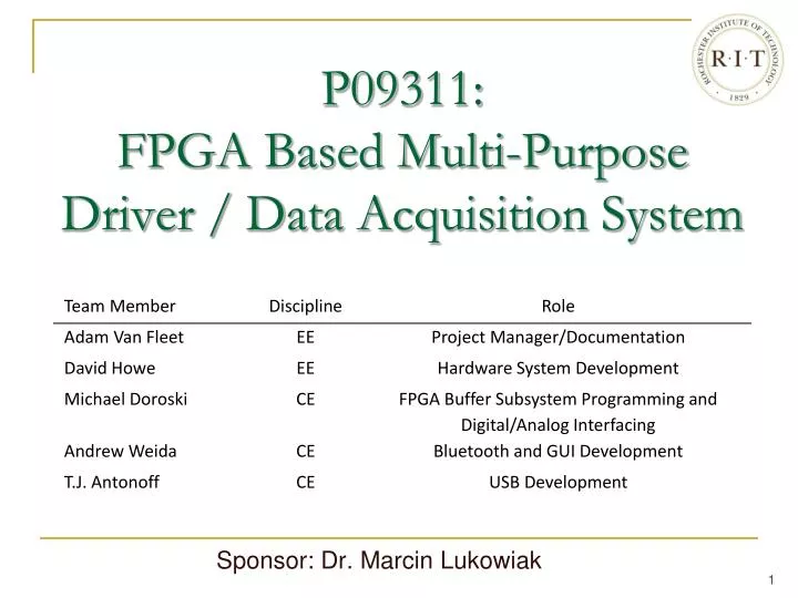
P09311: FPGA Based Multi-Purpose Driver / Data Acquisition System. Sponsor: Dr. Marcin Lukowiak. Project Description.

E N D
P09311: FPGA Based Multi-Purpose Driver / Data Acquisition System Sponsor: Dr. Marcin Lukowiak
Project Description • Goal: Design and implement a functional FPGA-based interface for the multi-purpose driver/data acquisition system. The interface must allow for data acquisition via USB and Bluetooth communication interfaces. • Utility: The project is to be utilized in Robotics and ASIC testing for research at the Rochester Institute of Technology.
High Level Customer Requirements • System • Utilizes FPGA interface. • Capable of transferring data via Bluetooth and USB communication channels. Option for Ethernet and Wireless communication channels. • Infinite sampling time desired (data streaming). • GUI displays data transfer statistics. • Text-file format for data storage.
Hardware Implementation Windows-Based PC ASIC or Robotics Input P08311 DAQ Board DLP-USB245M USB Adapter Parani ESD210SK Bluetooth Dev. Kit Spartan-3 FPGA
Top Level Architecture Design Control Unit FPGA USB 8 Mbps Input Conditioning Output Subsystem USB Data Routing Logic USB FIFO USB Cable DAQ PC Serial Output Conditioning Input Subsystem UART Tx Tx Bluetooth Wireless Rx Rx RS232 200 kbps Bluetooth Modules
Product Development Process Phase • Phase 0: Planning • Phase 1: Concept Development • Phase 2: System Level Design • Phase 3: Detailed Design • Phase 4: Testing and Refinement
Concept Summary Theory: The buffers can only empty as fast as the communication channel allows, but can load as fast as we choose. The buffer size is 216kb. The length of time for which we can transfer data is equal to the total memory size (216 kb) available, divided by the rate the memory is filled (Input Rate – Output Rate). Therefore, if the output rate is greater than the input rate, we can transfer information for an infinitely long period of time.
Concept Summary (Bluetooth) The Bluetooth device can only handle theoretical bit rates of 330 kb/s, limited by baud rate, and is seeing 200 kb/s in testing. Under full load, over 6 Mb/s is required. Therefore, the BT device will not be sufficient for data transfer under full load. 8
Concept Summary (USB) The USB system allows for an 8 Mb/s transfer rate, thus the buffer is never filled and data transfer can be streamed (infinite time length). Under full load, the maximum output rate required for streaming is 6,724 kb/s. 9
Design Summary The packet structure is broken down into: -MSB (B7): Determines if data is Analog or Digital -B6 to B4: Used to reassemble data on PC side -LSB’s (B3 to B0): Contain the data from DAQ or PC If the top nibble is set to ‘1111’, the last 4 data bits determine which analog channel the data is being received from.
Analog I/O Testing A 3.3Vpp sin wave is fed to the analog inputs of the DAQ, then through the Spartan-3 FPGA. The analog outputs are as shown. It is noted that as the frequency approaches 1kHz (left), the signal begins “stair-stepping”, as seen in P08311’s work. As the frequency increases to 2kHz and above (right), the stepping becomes much more apparent.
Digital I/O Testing A 1.5Vpp square wave is fed to the digital inputs of the DAQ, then through the Spartan-3 FPGA. The digital outputs are as shown.
Status of Design • Bluetooth System • Meets customer specifications • USB System • In system-level debugging to achieve customer specifications. • Graphical User Interface • Meets customer display specifications • Accurately depicts transfer rate and connection settings, allows for file selection. • Under budget of ~$500 • Schedule: 2 weeks behind schedule on USB, Bluetooth on schedule, ahead of schedule on GUI Interface.
Unresolved Issues • Bluetooth limited by memory size • Baud rate allows for 360kb/s max. transfer rate • 16 Mb additional memory requires project rework • USB Transmission Errors • Digital Output 2 stuck at ‘1’ • May require a new IC chip • Analog Data Transfer • Signals misrouted, likely due to timing errors. 15
MSDII Project Milestones • 4/03 – Concept Review • 4/10 – Finalize Design, Review System Concept • 4/20 – Subsystems Finalized, Begin Test & Debug • 5/05 – Entire System Finalized, Begin Test & Debug • 5/08 – Finalize and Submit Documentation • 5/15 – Project Review • 5/18 – Field Demo and Project Wrap-up
Q&A Questions?