Download
1 / 34
340 likes | 506 Views
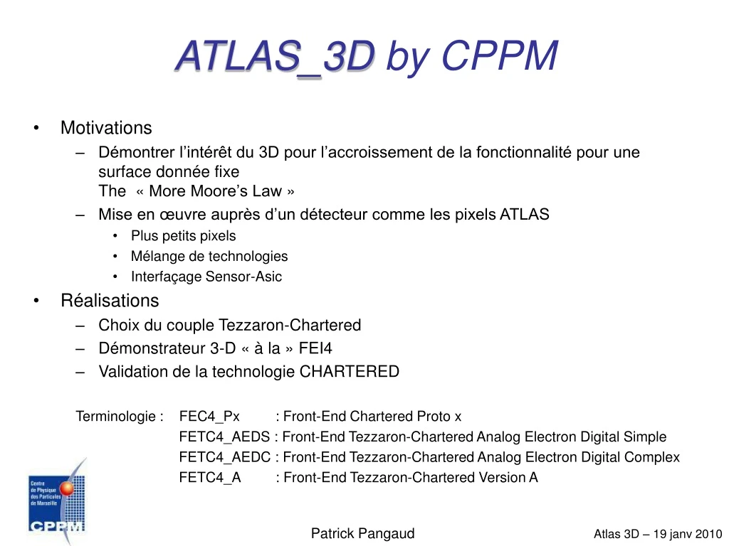
ATLAS_3D by CPPM. Motivations Démontrer l’intérêt du 3D pour l’accroissement de la fonctionnalité pour une surface donnée fixe The « More Moore’s Law » Mise en œuvre auprès d’un détecteur comme les pixels ATLAS Plus petits pixels Mélange de technologies Interfaçage Sensor-Asic

E N D
ATLAS_3D by CPPM • Motivations • Démontrer l’intérêt du 3D pour l’accroissement de la fonctionnalité pour une surface donnée fixeThe « More Moore’s Law » • Mise en œuvre auprès d’un détecteur comme les pixels ATLAS • Plus petits pixels • Mélange de technologies • Interfaçage Sensor-Asic • Réalisations • Choix du couple Tezzaron-Chartered • Démonstrateur 3-D « à la » FEI4 • Validation de la technologie CHARTERED Terminologie : FEC4_Px : Front-End Chartered Proto x FETC4_AEDS : Front-End Tezzaron-Chartered Analog Electron Digital Simple FETC4_AEDC : Front-End Tezzaron-Chartered Analog Electron Digital Complex FETC4_A : Front-End Tezzaron-Chartered Version A
FEC4_P2 : Status Remember : P2 from P1 • Optimization of Rad-Hard block and SEU tolerance blocs • Optimization of Analogue part vs Chartered Technology • But to follow the IBM release FEI4_P1 chip, we kept the same functionalities • Reduce the pixel size to 125µm Plan • Analog Pixel and analog functions • Global register • Digital Buffers • SEU latch • Next … FEC4_P1 : submitted in Fev 2009 FEC4_P2 : submitted in Nov 2009
FEC4 : Pixel overview ( size 50 x 166) From FEI4_P1 : Basically Technology translation from IBM to Chartered FEC4_P2 : Optimization of analog part and a new SEUlatch FEC4_P2 : Optimization of analog part and a second new SEUlatch • FEC4_P1 • FEC4_P21st SEU LATCH version • FEC4_P22nd SEU LATCH version
FEC4_P2 : Main changes in analogue pixel • The objectives were : • Not to change the structure • Simulate and adjust size of transistors
FEC4_P2 : Preamplifier • FEC4-P1 : • MN2 : 3µ/200n, nf=2, nmos_1p5_lvt • T21 : 6,25µ/300n, nf=2, nmos_1p5_nat • FEC4-P2 : • MN2 : 5,5µ/300n, nf=1, nmos_1p5_nat • T21 : 5,5µ/300n, nf=2, nmos_1p5_nat For Process variation : Better behavior with the same kind of transistor…
FEC4_P2 : Amplifier2 only 1 transistor (not 2 in series) with the same equivalent size To deal with increased Vt and to improve the linearity : Nf = 4 To increase the linearity : Bulk and source connected
FEC4_P2 : Simulation results typical process • linearity : • Noise from 60 e- to 200 e- depending on : • the process case • the capacitor value of the sensor (from 0 to 400fF) • The sensor current (from 0 to 100nA) preampli ampli2 preampli ampli2
FEC4_P2 : Global Register • Due to a defect working after irradiation, we decided to replace the SEU_LATCH cell by a LATCH Standard Cell from ARM.
Arm latch Port definition G : Load signal, the latch hold signal from DFF while the load signal is”0”. SN : Connect with a TIETHL. So the state always is “1”. RN : Clear signal. Connect it with an ‘Not gate’. So the ltchclr is high positive. D : Connect with DFF’s output ‘Q’. Q : The output of latch. Follow by a buffer. QN : Not used. FEC4_P2 : Global register cell Functions:
FEC4_P2 : layout of the Global register cell • 49.1u*82.3u of FEC4_P1 per 16 cell • 49u*82.3u of FEC4_P2 per 16 cell
FEC4_P1 : The Digital output buffer Fist stage, N: 0.44/0.14 P: 1.25/0.14 Second stage, N: 4.5/0.14 P: 13.5/0.14
FEC4_P2 : The Digital output buffer Fist stage, N: 4.625/0.13 P: 12/0.13 Second stage, N: 13.875/0.13 P: 36/0.13 Wellguardring for PMOS Enclosed Layout Transistor Guardring for NMOS
FEC4_P2 : Simulation results of the Digital output buffer Frequency of the input signal: 1/20ns (50MHz). Mode transistors: typical. Load capa = 10p. P1 P2 rise time: 1.786ns, fall time: 1.657ns rise time: 4,494ns fall time: 5,341ns
FEC4_P2 : More simulation results of the Digital output buffer
FEC4_P2 : SEU Latch in Pixel cell • Some ideas… • Optimization of the SEU Latch block • New layout • With and without ELT • Try the Triple Nwell • But only new layout and with and without ELT have been implemented
FEC4_P2 : SEU_LATCH (DICE) version 1 Added buffers at the inputs and outputs and load. Removed the Reset function. Linear Transistors used + guardring All corners simulation are OK
FEC4_P2 : SEU_LATCH (DICE) version 2 Added buffers at the inputs and outputs and load. Removed the Reset function. Replaced the Load switch by a Tgate ELT Transistors used + guardring All corners simulation are OK
FEC4_P2 : SEU_LATCH (DICE) version 3 Added buffers at the inputs and outputs and load. Removed the Reset function. Add Triple well and removed the Dual function ELT Transistors used + guardring Very bigger cell Not implemented. Not enough time ….. But very exiting approach
Current mirrors at the output of global DAC : L is increased (for a small improvement of matching and noise) (for example 1µ/1µ becomes 1µ/4µ…) Analogue buffers : → Not enough time to design a real output buffer. → Layout is drawn with enclosed NMOS. Layout correction For FEC4-P1, suba, subd, gnda and gndd are not correctly separated. → This is corrected for P2. PADs ring : new approach (the same used for FETC4) → suba and subd are separated from gnd and sub of ESD protection. → use of dedicated PADs for VDDAIO, VDDDIO and GNDAIO, GNDDIO (PADs power). FEC4_P2 : Other changes
FEC4_P2 : Conclusion …. • Optimization of design : OK • Repaired Test transitors : OK • Checked the ESD Pads : OK • Reduced the pixel size : NOK • Added a real analog buffer : NOK Awaiting test results (dies arrived previous week)
26mm 31mm FETC4_xx : MPW 3D-Fermilab Technology : Chartered 0,13µm LP + Tezzaron SuperContact ILC ATLAS LBNL
FETC4_xx : ATLAS Band -C SEU-3D SEU-3D FETC4-AE FETC4-DS TSV Daisy Chain + BI TSV vs Transistors Contraintes Mécaniques DFF + Trans + Cap TSV vs Transistors + Capacités
FETC4_xx : ATLAS Band -D OmegaPix Digital OmegaPix Analog FETC4-AE FETC4-DC TSV vs Transistors Capa TSV avec Bump TSV vs Transistors
FETC4_xx : LBNL- Fermilab band -G FETC4-AH FETC4-DS
FETC4_xx : 3D ATLAS projets • FETC4 –AE (CPPM) : pareil que FEI4_Proto1, mais en Chartered 0,13LP • FETC4-DS (CPPM) : Shift Register + compteur +readout data. "Drum registers" • FETC4-DC (Bonn-CPPM) : Lecture à double colonnes "à la FEI4" • FETC4-AH (LBL-CPPM): pareil que FEI4_Proto1 mais avec collection de trous. • SEU-3D (CPPM) : circuit numérique résistant au SEU " à la FEI4" • Multiples structures de tests (CPPM) • Daisy chain des TSV + BI (avec mesure de la résistance) • Capacités des TSV avec ou sans BackMetal, avec ou sans Bump • Transistors de test (Linéaire et ELT) proches des TSV • Effets de stress mécaniques sur les composants (Trans, Capa, Res, DFF)
FETC4_A • Motivation of a 3D-IT approach in HEP • smaller pixels and more functionality by pixel • Mixed technologies • Replacement for pixel bump bonding (Finer pitch bonding? Lower cost bonding?) Higher performance pixels detectors • Motivation of using Tezzaron-Chartered technology • Seems the only low-cost foundry at this time • Large reticule (26 mm x 31 mm) • Chartered (2D) MPW
FETC4_A • Organization • Same FEI4_A specification but with half-size pixel • Dedicated collaboration ‘à la’ FEI4_A. • Most important blocks should be implanted • Dedicated Blocks prototype • Prototype approach by using Chartered MPW
FETC4_A : Tezzaron-Chartered in HEP • Tezzaron : • Via first. • Super-Contacts (Through Silicon contacts) are formed before the BEOL of Chartered technology. • Back-side metal for bonding (after thinning). • 2 wafers (tier 1 and tier 2) are stacked face to face with Cu-Cu thermo-compression • Chartered: • 0.13LP technology with standard and low VT transistors. • Zero Vt transistors. • Deep nwell nmos. • I/O transistors for 1.8 to 3.3V operation. • MiM capacitor (single mask : 1fF/µm²). • 5 levels of metals and a redistribution of Top metal layer (M6) for bonding. • A 26 x 31 mm reticule size. 3D assembling of 2 tiers (T1 and T2)
FETC4_A : specifications To be compatible with FEI4_A sensor
Which blocks into T1/T2 ?? From FETC4_P1 ( to be finalized) To be synthesized with ARM cells To be developed ( 2D MPW to validate them) FETC4_A : building blocks Same FEI4 blocks, but only essential blocks, first.
CAD tools Cadence IC6.1.4 Last 0.13LP Chartered PDK Cliosoft Calibre 2009 Customized ARM cells Chip development approach The same organization than FEI4_A Shared project Fundamental blocks would be implemented. 2D Chartered MPW run to validate new cells. FETC4_A : organisation
FETC4_A : Chartered MPW 2010 FEC4_P1 and FEC4_P2 made in 2009, to validate the technology’s translation FEC4_P3 could validate more functionalities closed the FEI4_A final design FEC4_P3 Next submission dates
? 21x20 mm ATLAS 21x20 mm ATLAS FERMILAB MPW_2 ATLAS or CMP MPW_2 FETC4_A : 3D-run Submission The FETC4_A development could be start soon. The team can grow later, but the design strategy should be fixed before. Realistic schedule to be defined according to the design’s team