Download
1 / 34
350 likes | 574 Views
Lecture 4-4 Buses and Other Interfaces. Buses I/O interfaces in detail USB Next Lecture Memory system. BUSES. Provide a common communication path for the transfer of data Include lines to support interrupts and arbitration

E N D
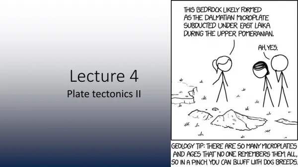
Lecture 4-4Buses and Other Interfaces • Buses • I/O interfaces in detail • USB • Next Lecture • Memory system
BUSES • Provide a common communication path for the transfer of data • Include lines to support interrupts and arbitration • A bus protocol: a set of rules that governs the behavior of the devices connected to the bus and when to place information on the bus, assert control signals, etc … • Three sets of wires: data, address and control lines • Control signals specify • whether a read or a write operation is to be performed, R/W: read when set to 1 and write when set to 0 • Timing information : times at which the processor or the I/O device can place data on the bus or receive data from the bus • Several schemes have been designed for the data transfers grouped under two categories: synchronous and asynchronous • In any transfer operation, one device plays the role of master (or initiator and initiates the transfer by issuing a read or a write) • Normally the processor acts as the master, but other devices with DMA capabilities may become bus masters
Single Cycle Transfer time Bus clock Address and command data t0 t1 t2 Bus cycle • Single cycle transfer results in a simple design for the device interface • Limitations • Because the transfer has to be completed within one clock cycle, t2-t0 must accommodate the longest delay on the bus for the slowest device • The processor has no way of determining whether the target has actually responded
Multiple Cycle Transfer • To overcome the limitations of single cycle bus transfer, most buses incorporate control signals that represent a response for the device (called Slave-ready) • Make it possible to adjust the duration of the transfer time 2 3 4 1 clock Slave-ready data Address Master command
Multiple Cycle Transfer Example • During clock cycle 1, the master sends address and command information on the bus, requesting a read operation • The following active edge of the clock, the slave makes a decision to respond and begins to access the requested data • Data is placed on the bus on clock cycle 3, at the same time the slave asserts a control signal call slave-ready • The master which has been waiting for this signal reads the data into its input buffer at the end of clock cycle 3 • The slave-ready is an acknowledgment from the slave to the master that valid data was sent • The slave-ready allows the duration of the bus transfer to change for other devices • If the target device does not respond at all, the master waits for some predefined maximum number of click cycles and then aborts the operation
Asynchronous Bus Data Read Address and command Master-ready Slave-ready Data t0 t1 t2 t3 t4 t5 Bus clock cycle
Asynchronous Bus Data Write • Processor places data, address and command information on the bus • Processor activates master-ready • The target device decodes the address, strobes the data into its buffer and indicates so by setting its slave-ready signal • Remaining steps are similar to the read operation Address and command Data Master ready Slave ready t1 t2 t3 t4 t5 t0 Bus clock cycle
Computer buses • Computer buses are standards that allow many manufactures to design computer components for different computers • Buses specify • The hardware – number of pins, function of each pin, connector type • The protocol – the speed of data transfer, the the timing of the signals, the arbitration method when more than one card need to use the bus • A bus bridge is used to translate between standard bus signals and CPU bus signals
Bus Bridges Front Side Bus
Interface Circuits • An I/O interface does the following • Provides storage buffer for data • Contains flags that can be accessed by the processor to determine whether the buffer is full or empty • Contains address decoding circuitry to determine when it is being addressed by the processor • Generates the appropriate timing signals required by the bus control scheme used • Performs any format conversion (e.g. parallel – serial)
Keyboard Interface • When a key is pressed, its switch is closed and establishes a signal • This signal is translated into an ASCII code • Push button switches can bounce • Either use a debouncing circuit or solve the bouncing problem in software • When a key is pressed, the valid signal changes from 0 to 1 • The ASCII code is loaded into DATAIN and SIN is set to 1 • SIN is cleared when the processor reads DATAIN
Circuitry for the Keyboard Interface • The output lines of DATAIN are connected to the bus through tri-state drivers • Address decoder selects the input interface when the high order 31 bits of an address correspond to the address assigned to the interface • Tri-state drivers are turned on when the processor issues a read with an address that selects this device • A0 determines whether the status or the data is to be read when ready (master-ready) is active • The handshake is accomplished by activating the accept signal (slave-ready) when either the read status or read data is one.
Display Interface • When the display is ready to accept another character, it asserts the Idle signal, which causes SOUT to set to 1 • The processor stores a new character into DATAOUT, which causes SOUT to set to 0 • The I/O interface then places a new character on the data lines for the display and activates the Valid signal • The display negates the Idle signal and starts displaying the new character • This causes the interface to deactivate the Valid signal Display
Circuitry for the Display Interface Display data
Combined Keyboard I/O Interface • The overall address is selected by the high order 30bits of the address • Bits A1 and A0 select one of the three addressable locations in the interface: two data registers and one status register • The status register contains SIN and SOUT SOUT
Serial Interface • Used to connect devices that require transmission of data one bit at a time • Transformation between parallel and serial formats can be done with shift registers
PCI (Peripheral Component Interface) bus • PCI bus is popular for PCs • PCI is a synchronous bus architecture with all data transfers being performed relative to a system clock (CLK). • PCI connector has 94 pins • The maximum clock rate is 66 MHz • Majority of today's personal computers implement a PCI bus that runs at a maximum speed of 33 MHz (original PCI clock rate)
PCI-Express (PCI-E) • To overcome PCI’s noise, cost, poor frequency scaling problems, PCIe takes a serial approach • Each link is composed of one or more lanes, and each lane is capable of transmitting one byte at a time in both directions at once, i.e., full-duplex communication • A single lane is capable of transmitting 2.5Gbps in each direction, simultaneously
PCI-E • Feature: the ability to aggregate multiple individual lanes together to form a single link • A link that's composed of a single lane is called an x1 link; a link composed of two lanes is called an x2 link; a link composed of four lanes is called an x4 link, etc. • PCIe supports x1, x2, x4, x8, x12, x16, and x32 link widths
Nvidia’s SLI Video Cards • Scalable Link Interface • Two PCI-E ultra graphics cards running in an SLI configuration
Nvidia’s SLI Video Cards • 3D rendering involves moving a lot of data around, very quickly, between the video card, the CPU, and main memory. • Two video cards placed in a pair of x16 slots will have high-bandwidth pipes connecting them to each other, to main memory, and to the CPU. • They can use all of that bandwidth to cooperate on rendering chores at a level that wouldn't have been feasible with previous bus technologies • They need to be plugged into a connector slot that supports at least 16 lanes.
HyperTransport • HyperTransport interconnect technology is a high-performance, high-speed, high-bandwidth, point-to-point link that provides the lowest possible latency for chip-to-chip and board-to-board links • HyperTransport 3.0 with clock freq. up to 2.6 GHz delivers a maximum aggregate bandwidth of 41.6 GB/s • HyperTransport is fully compatible with legacy Peripheral Component Interconnect (PCI), PCI-X and PCI Express technologies. • HyperTransport Consortium • http://www.hypertransport.org/
HTX • HyperTransport-based, slot-type, direct-connect interface between peripheral subsystems and system CPU(s)
Universal Serial Bus (USB) • USB is an asynchronous serial port • USB uses half duplex transfer • It provides point to point connection • It provides an instant, no-hassle way to connect a new digital joystick, a scanner, a set of digital speakers, a digital camera, or a PC telephone to their computer. • USB 2.0 Transfers 480 Mbit per second • Adding an old-fashioned peripheral device used to be cumbersome • First you must find out which port to use. • You may have to open your PC to install an add-in card and set DIP switches. • You may need to set IRQ and other parameters to configure the computer
Good Features of USB • A simple low-cost flexible mechanism • USB allows "hot-swapping” • Just plug it in and go! • Don't need to shut down PC to attach or remove a peripheral. • The PC automatically detects the peripheral and configures the necessary software. • USB lets users to connect many devices (peripherals) at one time • USB hubs let you "daisy chain" multiple devices together • USB distributes electrical power to many peripherals • USB lets the PC automatically sense the power that's required and deliver it to the device
USB cable • VBUS is the power source • GND is ground • D+ and D- are differential data lines • Half-duplex VBUS VBUS D+ D+ D- D- GND GND
USB devices • A USB system is described by 3 definitional areas: • USB host • USB interconnect network • USB devices • USB devices connect to the USB host • The USB physical interconnect network is a tiered star (tree) topology • A hub is at the center of each star • Each wire segment is a point-to-point connection • between the host and a hub or function, or • a hub connected to another hub or function.
USB Connection Uses a Tree Topology At most 7 tiers including Host
USB Host • The USB host (usually the PC) interacts with USB devices through the Host Controller • The host is responsible for the following: • Detecting the attachment and removal of USB devices • Managing control flow between the host and USB devices • Managing data flow between the host and USB devices • Collecting status and activity statistics • Providing power to attached USB devices
USB Functions • Each USB function contains configuration information that describes its capabilities and resource requirements • Before a function is used, it must be configured by the host • This configuration includes allocating USB bandwidth and selecting function-specific configuration options • Examples of functions include the following: • A human interface device such as a mouse, keyboard, tablet, or game controller • An imaging device, e.g., scanner, printer, or camera • A mass storage device such as a CD-ROM drive, floppy drive, or DVD drive • Reference: http://www.usb.org/developers/docs/
EIDE Disk Drive Interface • 16-bit Parallel interface for disk drives • It was originally conceived as PC/AT Attachment • Integrated Drive Electronics (IDE) • Enhanced IDE (EIDE) • allowed the support of drives having a storage capacity larger than 528 megabytes, up to 8.4 gigabytes • Started with PIO (Programmed Input/Output) • Later DMA and Ultra DMA (UDMA) greatly reduced the amount of processing time the CPU had to use in order to read and write the disks. This is possible because DMA and UDMA allow the disk controller to write data to memory directly, thus bypassing the CPU
Serial ATA (SATA) • A computer bus technology primarily designed for transfer of data to and from a hard disk. It is the successor to the legacy Advanced Technology Attachment standard (ATA). This older technology was retroactively renamed Parallel ATA (PATA) to distinguish it from Serial ATA. Both SATA and PATA drives have the low level control integrated into the drive but the term IDE is usually restricted to parallel ATA drives. • Serial ATA uses 8B/10B encoding at the physical layer • Low Voltage Differential Signaling (LVDS) is used • SATA 1.5 Gbit/s • Run at 1.5 gigabits per second (Gbit/s) • This encoding scheme has an efficiency of 80%, resulting in an actual data transfer rate of 1.2 Gbit/s, or 150 megabytes per second (MB/s)
SATA II • Soon after SATA's introduction, enhancements were made to the standard. A 3 Gbit/s signaling rate was added to the PHY layer, offering up to twice the data throughput. Like SATA 1.5 Gbit/s, SATA 3.0 Gbit/s uses 8B/10B encoding, resulting in a maximum data transfer rate of 2.4 Gbit/s or 300 MB/s for the wire. However, hard drives cannot supply data nearly at these speeds, so the actual speed depends on the hard disk. • Future design: SATA 6.0 Gbit/s