Download
1 / 27
270 likes | 275 Views
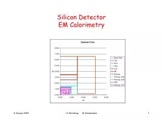
The CLEO-III Silicon Detector. Richard Kass The Ohio State University Kass.1@osu.edu Vertex 2001 September 24, 2001. Introduction Detector Design/Goals Initial Operating Experience Longer term performance/radiation damage Summary/Conclusions.

E N D
The CLEO-III Silicon Detector Richard Kass The Ohio State University Kass.1@osu.edu Vertex 2001 September 24, 2001 • Introduction • Detector Design/Goals • Initial Operating Experience • Longer term performance/radiation damage • Summary/Conclusions Richard Kass, Ohio State University
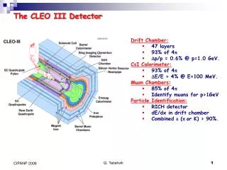
Located at CESR, symmetric e+e- collider at ¡(4S) resonance New RICH particle ID. CLEO achieves > 4 s K/p separation over full momentum range New Drift Chamber with same Dp/p and smaller tracking volume to accommodate IR Quads and RICH. New large 4 Layer SI Detector CLEO-III Detector Richard Kass, Ohio State University
CLEO Physics Program • 1990-1999: CLEO-II+II.5 collected ~10 fb-1 on the ¡(4S) • 2000- June 2001: CLEO-III collected ~ 9 fb-1, 70% on the ¡(4S) • November 2001-2002: CLEO-III will take data on the ¡(1S), ¡(2S), ¡(3S) • 2003-5: CLEO will operate in the 3-5 GeV energy range. A proposal has been written. Recent t-charm workshop: http://www.lns.cornell.edu/public/CLEO/CLEO_C Richard Kass, Ohio State University
Silicon Detector Operation Installation February 2000 Commissioning March-July 2000 òL=590 pb-1 Physics Data Taking July 2000-June 2001 òL = 9 fb-1 @ ¡(4S) Richard Kass, Ohio State University
CLEO-III Event Richard Kass, Ohio State University
CLEO III Silicon DetectorDesign Goals • Integrated tracking system SI measures z, cotq, Drift chamber measures curvature Both detectors measure f. • Tracking of low momentum p’s require small radiation length of SI detector. < 2% X0 achieved! • Also required for good tracking: • Signal-to-noise larger than 15:1 in all layers • Resolution better than 15 mm in r-f, 30 mm in z for tracking and secondary vertices (t and D-mesons only , B’s have no boost) • 93% solid angle coverage (same as our drift chamber) Richard Kass, Ohio State University
Mechanical Design constraints • Tight mechanical constraints on SI3 detector: • 93% solid angle coverage • Front end electronics mounted on support cones outside tracking volume puts severe constraints on electrical design. • CVD Diamond v-beams for mechanical support of silicon ladders 200-300 mm thick, < 0.1 X0 Richard Kass, Ohio State University
Mechanical Design (0.26% X0) 61 half ladders with 447 silicon Wafers Layer 4 is 53 cm long, Layer 1=16cm Richard Kass, Ohio State University
Silicon Sensor • Double-sided silicon wafer by Hamamatsu • 2 x 511 channels, wafer 53.2 x 27 x 0.3 mm • Strip spacing 50 mm r-f, 100 mm z. • Ladder length requires low strip capacitance. 9 pF in p and n achieved, • N-side with pstops, atoll design, pstops punch-through biased. • P-side is double metal side. Hourglass design of metal layer overlap. • AC coupling capacitor and bias resistor on separate chip • Radiation damage constant(surface damage) 5 nA / kRad / (exposed) cm2 N-side = rphi P-side = z Richard Kass, Ohio State University
Readout Chain Modular Design of Wafers and Hybrids Richard Kass, Ohio State University
Front-End Electronics • RC chip (CSEM) • RC chip hosts bias resistor and ac coupling capacitor • Operation voltage of RC chip 0-60 Volts • Front-End Electronics (Honeywell Rad Hard) • PreAmp gain 40mV/MIP, output 200mV/MIP • Shaping time variable between 0.7 - 3.0 msec • FE noise performance optimized with SPICE • ENC = 145 e + 5.5 e /pF measured • BE Chip (Honeywell Rad Hard) • 8 bit ADC, comparator and FIFO, on-chip sparsification Richard Kass, Ohio State University
Hybrid Board RC BE FE Detector Richard Kass, Ohio State University
Hybrid Board • 122 Hybrids, 125,000 readout channels • Double-sided board carries 8 sets of RC, FE and BE chips • Five electronics layer on BeO core • ~60 surface mount parts, 24 chips and 2400 encapsulated wire bonds • Noise performance on fully populated BeO-boards < 300 ENC • < 4 Watt power consumption / hybrid • cooling through thermal contact with support cones Richard Kass, Ohio State University
Slow Control • Hybrid voltages controlled by port cards • Port cards connected to DAQ, slow control and power system • Slow Control system monitors voltage, current, and temperature levels and sets hybrid voltages • Slow control process resides in a single crate CPU • Communication with Power crates through VME repeater boards • SI detectors turn off if slow control process dies (time-out function of power distribution boards) Richard Kass, Ohio State University
Power Supply System • Linear power supplies chosen for low noise performance • Power distribution boards in VME crates, power feed-in through J3 back plane connector • 4 hybrids powered per board • Analog and digital section isolated through opto-couplers • Additional monitoring software runs in CPU on board Richard Kass, Ohio State University
Initial Silicon Detector System Performance • Signal-to-noise, Situation right after installation (July 2000) Signal/Noise Noise (100 e) Layerr-phi z r-phi z 1 27.9 34.4 6.1 6.1 2 29.9 37.4 5.9 4.4 S/N >19, 3 19.4 27.3 8.2 5.7 Noise 400-600 e- ENC 4 20.1 22.6 8.2 6.5 • Frontend electronics works fine, low noise, common mode noise <400 e- • Stable power system hep-ex/0103037, to be published in NIM A Richard Kass, Ohio State University
x SI Ladder x x track PerformanceHit Resolution • Residuals from SI-hit extrapolation Residual r-f=13 mm , Z= 31 mm • Resolution = Residual / Ö (3/2) Resolution r-f=11 mm , Z= 25 mm Residual = 31 mm Residual = 13 mm Residual (50 mm) Richard Kass, Ohio State University
Detector Alignment • Ladder assembly relatively precise • Average sensor displacement 8 mm in r-phi, 10 mm in z • Most ladders are precisely positioned, but few moved within kinematic mounts by a several 100 mm. • Software alignment: work in progress Resolution so far 40 mm r-phi, 200 mm in z • Tracking resolution dominated by residual silicon misalignments Richard Kass, Ohio State University
Detector Alignment continued Residuals before Alignment After first Alignment Z0 Bhabhas w/o SI s =7000 mm with SI s =200 mm Richard Kass, Ohio State University
Radiation Sickness • Initially, efficiency in layer-1, r-f, was ~60%. Lower than expected But other layers (r-f, z) were ok • First hint at true nature of problem from high-statistics mapping of silicon hits. • r-f efficiency shows structure on the wafer. • Varying the detector/FE electronics settings within the possible range could not restore efficiency. Richard Kass, Ohio State University
Hit Map Study Hit Map, Layer 1 • 2D-Hit-map for first layer • 3 sensors per ladder with 2mm spacing • Half rings structures on sensors visible • Half rings could match full rings on original wafers Dead readout chains Wafer Sensor Sensor Half-Ring Structures Richard Kass, Ohio State University
Time Evolution Example: a Layer-2 Sensor • Problem(s) getting worse with time • Affected now: Layers 1+2 r-f Outer layers still ok, z-side still efficient • Most likely explanation: Radiation damage to silicon sensors. Exact mechanism unknown. Richard Kass, Ohio State University
Irradiation Studies • Original studies were performed ~5 years ago on pre-production sensors and concentrated mostly on detector current vs dose. • Small increase in detector current expected, mostly due to x-ray-induced surface damage. • Sensors and FE electronics were designed to be radiation hard (Mrad), expected to be operational for at least 10 years. • We observe the expected increase in detector leakage current, 1-2 mA per sensor so far. CESR’s radiation levels are only a little bit higher than expected. • Discussed situation with Hamamatsu • Detailed irradiation studies are underway….. Richard Kass, Ohio State University
Sr90 Source Test Compare CLEO III silicon wafer with SINTEF wafer Readout P-side using DC coupled Viking electronics Trigger readout using b’s that pass through silicon ----- 0krad ----- 4krad CLEO III detector ~ 15% decrease in M.P. SINTEF detector Richard Kass, Ohio State University
CERN Beam Test Readout single strip (P-side) Move along strip Use existing Si telescope Map out response of wafer Use 100 GeV pion beam 2-D map of pulse heights Region exposed To 4krad Sr90 M.P.= 67 Unexposed region M.P. = 77 Richard Kass, Ohio State University
LED and Synchrotron Radiation Tests Red LED probes surface IR LED and Synchrotron x-rays (16 keV) probe bulk Before irradiation LED’s scan across wafer (N-side) Move from strip to strip, constant position along a strip Ring structure Apparent in LED tests ! IR LED after 100 krad Red LED before irradiation Richard Kass, Ohio State University
Summary and Conclusion • CLEO has accumulated ~9 fb-1 of e+e- data. • In operation, FE electronics reached design goals: 400-600 e noise. • Signal-to-Noise and resolution goals were reached initially. • Silicon sensors show signs of radiation damage much sooner than expected. r-f side shows ring patterns on the sensors. • Studies underway to understand the damage mechanism. Richard Kass, Ohio State University