Download
1 / 10
100 likes | 199 Views
Multiscale modelling of sparking in CLIC components. F. Djurabekova , K. Österberg, H. Timko, A. Ruzibaev, A. Pohjonen, S. Parviainen, K. Nordlund, HIP; in close collaboration with Walter Wuensch and Sergio Calatroni (CERN).

E N D
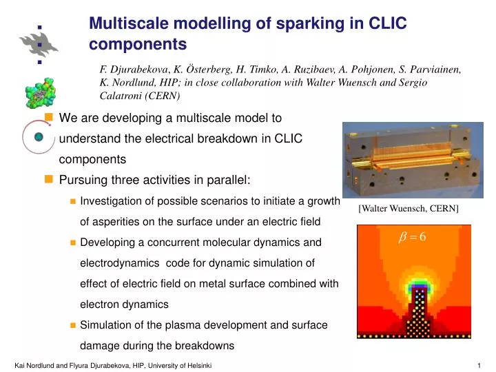
Multiscale modelling of sparking in CLIC components F. Djurabekova, K. Österberg, H. Timko, A. Ruzibaev, A. Pohjonen, S. Parviainen, K. Nordlund, HIP; in close collaboration with Walter Wuensch and Sergio Calatroni (CERN) • We are developing a multiscale model to understand the electrical breakdown in CLIC components • Pursuing three activities in parallel: • Investigation of possible scenarios to initiate a growth of asperities on the surface under an electric field • Developing a concurrent molecular dynamics and electrodynamics code for dynamic simulation of effect of electric field on metal surface combined with electron dynamics • Simulation of the plasma development and surface damage during the breakdowns [Walter Wuensch, CERN]
Dislocations as source of tip growth • We have shown that a void below a surface can act as a source for growth of protrusions and ejection of material [Pohjonen, Djurabekova, Nordlund, Fitzgerald, Phys. Rev. B (2010) submitted)]
Dislocations as source of tip growth • The growth can be understood in terms of the void emitting a series of prismatic dislocation loops that glid to the surface and cause growth there [Pohjonen, Djurabekova, Nordlund, Fitzgerald, Phys. Rev. B (2010) submitted)]
Algorithm for finding the charge on metal atoms due to the electric field. • Gauss law = 0Elocas a source of a charge estimation where Eloc is a local field near the atom surface. • Since the atoms belong to the surface they can be only partially ionized. ELOC • In the present algorithm: • the atoms are rectangular grid points, which are part of the same grid as for a Laplace solver • Problem: the discreteness of the Laplace solver -> presence of the tangential component of electric field. • Solution: only perpendicular to the atom surface components are taken into account. • the change of local density of atoms also affects the distribution of charge
Verifying algorithm for finding the charge on metal atoms due to the electric field, part 1. The accuracy of the discretization of the Laplace solution has been tested against an exactly solvable case -> agreement within a few %! ELOC [Djurabekova, Parviainen, Nordlund, Phys. Rev. E (2010) submitted)]
Verifying algorithm for finding the charge on metal atoms due to the electric field, part 2. Accuracy of the interatomic potential energy has been tested again quantum mechanical (DFT) calculations of the case of a single adatom on a tungsten surface Very good agreement! Agrees with experimental value for the critical field for field evaporation in W of about 50 GV/m! ELOC [Djurabekova, Parviainen, Nordlund, Phys. Rev. E (2010) submitted)]
Field increase at protrusions • Our model also reproduces the increase of the field strength around a hemispherically capped cylinder in excellent agreement with previous Finite Element Method calculations • Field strength increases less than linearly, in agreement with the literature Electric field enhancement Aspect ratio of tip
Electronic effects in MD • Heating depends on several electronic effects Escreened At the moment a 1D equation to handle the temperature raise due to the Joule heating is implemented into the parcas MD code Electron screening Electric current (resistive heating) Here electron thermal conductivity introduced explicitly according to the Wiedemann-Franz law Heatconduction
Resistive heating leads to necking in tips • Starting from a cylindrical tip, the Joule heating and desire of material to minimize surface energy (Rayleigh instability) leads to necking (thinning) below the maximum • First stage for atom or cluster emission that is needed for onset of plasma! [Parviainen, Djurabekova, Timko, Nordlund, Comput. Mater. Sci. (2010) submitted)]
Outlook • The validated ED-MD will be used in the electronic heating and dislocation dynamics simulations to use a realistic surface force model in them • Dislocation dynamics: the effect of temperature on the emission of dislocation and surface growth due to voids will be determined • Finite-size effects are studied to estimate a realistic time range for the melting of surface asperities • Study includes both cylinders on surfaces and isolated nanowires • 2D PIC model under development • The effect of the spatial and velocity distribution of bombarding ions on the surface damage as a result of plasma interaction with the cathode is being studied