Download
1 / 33
350 likes | 530 Views
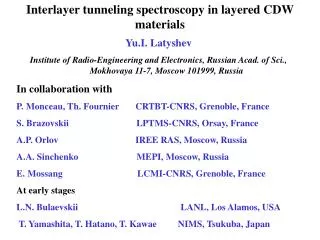
Interlayer tunneling spectroscopy in layered CDW materials. Yu.I. Latyshev Institute of Radio-Engineering and Electronics, Russian Acad. of Sci., Mokhovaya 11-7, Moscow 101999, Russia In collaboration with P. Monceau, Th. Fournier CRTBT-CNRS, Grenoble, France

E N D
Interlayer tunneling spectroscopy in layered CDW materials Yu.I. Latyshev Institute of Radio-Engineering and Electronics, Russian Acad. of Sci., Mokhovaya 11-7, Moscow 101999, Russia In collaboration with P. Monceau, Th. Fournier CRTBT-CNRS, Grenoble, France S. Brazovskii LPTMS-CNRS, Orsay, France A.P. Orlov IREE RAS, Moscow, Russia A.A. Sinchenko MEPI, Moscow, Russia E. Mossang LCMI-CNRS, Grenoble, France At early stages L.N. Bulaevskii LANL, Los Alamos, USA T. Yamashita, T. Hatano, T. Kawae NIMS, Tsukuba, Japan
OUTLINE • Introduction to interlayer tunneling. • Mesa fabrication and experimental technique. • CDW gap spectroscopy. • CDW amplitude soliton spectroscopy. • Threshold for interlayer tunneling. • CDW spectroscopy at high magnetic fields. • Conclusions
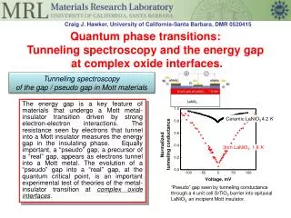
Introduction to intrinsic Josephson effects (IJE) and Josephson flux-flow (JFF) in layered HTS materials The amplitude of the OP is vertically modulated, while phases are coupled. One can expect both phase interference effect and quasiparticle tunneling. IJE - Josephson effects on naturally layered crystalline structure of layered superconductors I. Phase effects Early ideas in 70-s: W.E.Lawrence, S.Doniach 1971L.N. Bulaevskii 1973 Further development in 90-s, after discovery of HTS L.Bulaevskii, J.Clem, L.Glazman 1992 stationary IJE for short stacks L< 2J, J, = s c /ab~ 1m in Bi-2212 L L L s
First experimental evidence of IJE: R.Kleiner, P.Mueller et al. PRL 1992 R. Kleiner and P.Mueller PR 1994 They had junctions of big lateral size ~ 30 m and Fraunhoffer oscillations of critical current were not so clear Yu.I.Latyshev, N. Pavlenko, S-J.Kim, T.Yamashita ISS-99, Morioka Bi-2212 stack: L=1.4 m, s=1.5 nm, H=1.01 T
Josephson vortices Long stack, L>>J Josephson vortex (phase topological defect). No normal core. J. Clem and M.Coffey, PR 1990 Phase coherency is locally broken with appearance of JV at H>Hc1 Josephson-vortex lattice (JVL) L. Bulaevskii and J. Clem, PR 1991 Dense Josephson-vortex lattice ~103 Bcr~0.3T L. Bulaevskii, D.Dominguez et al. PR 1996 Dense lattice can move as a whole being driven by DC current across the layers
Josephson flux-flow regime Swihart velocity, velocity of electromagnetic wave propagation when the slowest mode (triangular lattice) ~0.1% c resonance occurs => flux-flow step Experiments Linear ff, low fields J.U Lee et al. 1995 ------------------------------------------------------------------ ff-step B1TYu. Latyshev, P. Monceau et al. Physica C 1997 ------------------------------------------------------------------ ff-step B<0.3T G. Hechtfischer et al. PR 1997 ------------------------------------------------------------------ ff-step 0.5<B<3.5TG. Hechtfischer et al. PRL 1997
The experimental ways to identify JVL (1) Shapiro step response in JFF regime to subterahertz external radiation. Coherent response of 60 elementary junctions Yu.Latyshev, M.Gaifullin et al. PRL 2001 with N=57
(2) Commensurate oscillations of Josephson flux-flow resistance in narrow mesas Commensurate boundary pinning of JVL w triangular lattice rectangular lattice H s w = 0, w= 1.8 m S. Ooi, T. Mochiku, K.Hirata, PRL, 2002 H s w = ½ 0, w=7.3; 18; 31m I. Kakeya, K. Kadowaki et al. 2004 T. Hatano et al. 2004
II. Quasiparticle tunneling over a gap: multibranched IVs, gap/pseudogap spectroscopy Yu.I. Latyshev et al.ISS Conf. 1999, Physica C, 2001; V.M. Krasnov et al. PRL, 2000, 2001
CDW interlayer tunneling spectroscopy: NbSe3 The elementary prisms are assembled in elementary conducting layers with higher density of conducting chains (shaded layers in a figure) separated by a double barrier of insulating prism bases. That results in a very high interlayer conductivity anisotropy a*/b ~ 10-3 at low temperatures compared with intralayer anisotropy c/b ~ 10-1. That provides the ground for interlayer tunneling spectroscopy of CDW layered materials..
FIB microetching method Yu.I. Latyshev, T. Yamashita, et al. Phys. Rev. Lett., 82 (1999) 5345. S.-J. Kim, Yu.I.Latyshev, T. Yamashita, Supercond. Sci. Technol. 12 (1999) 729. FIB machine Seiko Instruments Corp. SMI-9000(SP) Ga+ ions 15-30 kV Beam current : 8pA – 50 nA Minimal beam diameter: 10nm
stack Stacked structures fabricated from CDW materials by FIB methods NbSe3 mesa fabricated by double-sided FIB method (CRTBT-CNRS, Grenoble) TaS3 mesa fabricated by lateral FIB etching method (RIEC, Tohoku Univ.,Sendai) KMo6O17 mesa fabricated by lateral FIB etching method (Crystals were kindly provided by C. Schlenker and J. Markus, LEPES)
NbSe3: low temperature interlayer tunneling spectra Yu.I. Latyshev, P. Monceau, A.A.Sinchenko, L.N. Bulaevskii, S.A. Brazovskii, T. Kawae, T Yamashita,. J.Phys. A, 2003 Coexisting of both CDW gaps, zero bias conductance peak (ZBCP) 22 50-60 mV, 21 130-150 mV Consistent with STM, optics and low temperature ARPES data
22 (a) 21 Temperature evolution of the spectra Point contact spectra NbSe3-NbSe3 along the a*-axis A.A. Sinchenko et al., 2003 Stacked junction behaves as a single junction. We consider that as the weakest junction in the stack.
Zero bias conductance peak Bulaevskii theory of coherent tunneling of the ungapped carriers L.M Bulaevskii, JETP Lett. 2002. Coherent tunneling implies the conservation of particle in-plane momentum in the process of tunneling. This is necessary because the pockets represent some localized small parts of the Fermi surface and electron momrntum should not be scattered beyond the pockets by tunneling from one layer to another. The width of ZBCP characterizes the energy uncertainty for the state characterized by momentum p. Fitting parameters: eff = 0.25 mV, sc= 0.13 mV, N=30, m*=0.24 me, (T) was taken from the paper of N.P.Ong PRB 1978 for dI/dV
Intragap states: NbSe3 There are two new features inside the CDW gap with characteristic energies Vs ~2/3 and Vt ~ 2/10
Amplitude solitons in the incommensurate CDW (ICDW) The order parameter in the ground state is 0 =A cos (Qx + ) with Q the CDW wave vector Q = 2kF and the arbitrary phase in the ICDW state and A=const. That means that ground state is degenerated with respect to A -A. That leads to the possibility of configuration with accepting of one electron and formation of new ground state with A=tanh (x/0) called amplitude soliton (AS). AS is a self-localized state with an energy Es= 20 /. S.A. Brazovskii, Sov. Phys.-JETP, 1980 This state is preferable since its energy is smaller than the lowest energy 0 of the free band electron by 0/3. The existence of ASs has been well documented for in dimeric CDW materials (polyacetilene or CuGeO3). However , for ICDW materials of higher order incommensurability as MX3 existence of ASs has not been reliably demonstrated yet.
Intragap CDW spectroscopy in NbSe3. (I) ZBCP is suppressed by temperature Temperature dependence at high temperatures T > Tp/2 CDW 1 Peak at Vs 2/3 for both CDWs, Scaling Vs and 2 is temperature independent!!! CDW 2
(II) ZBCP narrowed by magnetic field Soliton peak at low temperatures At high magnetic fields parallel to the layers, H//c T=4.2K Parallel magnetic field narrows ZBCP and soliton peak becomes clear Perpendicular magnetic field to the contrast broadens ZBCP
CDW gap spectroscopy: o-TaS3 Parabolic background substraction at high temperatures ICDW-CCDW transition at T 130 K
Schematic view of tunneling spectra NbSe3 o-TaS3 at CCDW amplitude solitons with accepting of one electron are forbidden
Threshold for interlayer tunneling Specially designed mesa oriented across the chain direction to avoid contribution of CDW sliding in connecting electrodes Set up Threshold behaviour is very clear
Threshold voltage scaling with CDW gap CDW 1 o-TaS3 CDW 2 Scaling with eVt 0.2 NbSe3
Threshold voltage scaling with Tp eVth 1.3 kTp
CDW dislocation lines (DLs) The energy ~ Tp is known as an energy of 3D CDW ordering. As known from structural measurements, above Tp transversal phase coherence of the CDW becomes lost. Therefore, Vt may be interpreted as phase decoupling between neighbour elementary layers. S. Brazovskii suggested that this decoupling occurs via successive entering in the “weakest” junction the set of dislocation lines. DLs appear as a result of share stress induced by electric field across the layers. Each DL is oriented across the chains in elementary junction and corresponds to the charge 2e per chain or entering of one unit of CDW period. DL can be considered as phase CDW vortex. There is also some similarity between Vtand Hc1 in superconductors. Electric field concentrates within dislocation core: dz~ 10Å i.e. that drops within one junction, L= p/Tp ~ 20. L~ 200 Å. For 1 m size junction one needs 5-10 DLs to overlap all the junction area and to have complete decoupling of neigbour layers. So one can expect multiple threshold for successive entering of a of DLs.
Threshold and staircase structure CDW 1 CDW 2
When dislocation cores start to overlap at high voltage bias all the voltage drops on a single elementary junction. That can explain puzzling equivalence of the behaviour of the stacked junction and point contact containing one junction.
Metal - insulator transition for interlayer conductivity in NbSe3 induced by high magnetic field Yu.I. Latyshev, P. Monceau, A.P. Orlov, A.A.Sinchenko, T. Fournier, E. Mossang , 2004 Colossal magnetoresistance at eV< 2, that can achieve 2 orders at H=25 T, some enhancement of the lower CDW gap by magnetic field Questions 1. Field induced CDW? One can expect then enhancement of lower Tp. 2. The ZBCP still survives and acquires step-like form. We will study this state in future experiments.
SUMMARY • The FIB technique has been adapted for fabrication of micron sized stacked junctions for interlayer tunneling spectroscopy of layered CDW`materials. • Using interlayer tunneling spectroscopy we identified the CDW gap and zero bias conductance peak (NbSe3) attributed to coherent tunneling of uncondensed carriers. • We found some evidence of an existence of amplitude soliton states inside the CDW gap for both materials, NbSe3 and TaS3, and for both CDW states in NbSe3. • We found a threshold and staircase structure for interlayer dynamic conductivity as a function of bias voltage. We associate a threshold with the nucleation of the first CDW dislocation line in the weakest intrinsic junction. The staircase structure is explained as a successive nucleation of a row of CDW dislocation lines. • We found that magnetic field perpendicular to conducting planes essentially suppresses tunneling density of states at eV<2 leading to a colossal magnetoresistance. That is a sort of metal-insulator transition mediated by magnetic field.