Download

1 / 24
240 likes | 249 Views
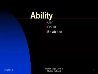
Why English is Important. English ability would save life English ability gives you opportunities http://www.youtube.com/watch?v=tcseWVNmda8 e.g. Job opening in TSMC http://www.tsmc.com/chinese/careers/jobs.html. http://www.youtube.com/watch?v=GT86iWiH2mI.

E N D
Why English is Important • English ability would save life • English ability gives you opportunities http://www.youtube.com/watch?v=tcseWVNmda8 e.g. Job opening in TSMC http://www.tsmc.com/chinese/careers/jobs.html http://www.youtube.com/watch?v=GT86iWiH2mI
What should you do to learn English in this class? • Read largely - preview textbook before class - review textbook and note after class • Increase your vocabulary • Invest your time to learn English regularly - Reading CNN, yahoo, newspaper - Listening radio youtube watching TV
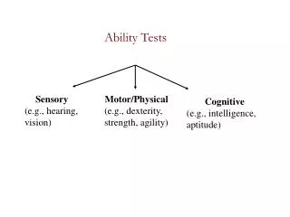
Ch.1 Introduction • Optoelectronic devices: • - devices deal with interaction of electronic and optical processes • Solid-state physics: • - study of solids, through methods such as quantum mechanics, crystallography, electromagnetism and metallurgy • Elemental semiconductors: • - Si, Ge, ..etc. • - indirect bandgap, low electric-optics conversion efficiency • Compound semiconductors • -III-V (e.g. GaN, GaAs), II-VI • -direct bandgap, high electric-optics conversion efficiency • GaAs, InP • - higher mobility than Si, Ge, • - energy band gap, Eg: 1.43 (GaAs), 1.35 (InP) • - most common substrate, used to grow up compound semiconductors
Band structure • Band structure: • - results of crystal potential that originates from equilibrium arrangement of atoms • in lattice - directed from potential model and electron wave equation (Schrodinger equation) time-dependent Schrodinger equation E: electron energy, φ:wave equation, m: electron mass, ħ: Plank constant
Wavelength (Bandgap) Engineering Reference article: http://www.tf.uni-kiel.de/matwis/amat/semi_en/kap_5/backbone/r5_1_4.html
Energy bandgap v.s. lattice constant • Constrains for forming compound semiconductors: • (1) requirement of lattice match, (2) availability of suitable substrates • GaAs and InP are most common substrates used to grow up compound semiconductors • (Note: InAs, InSb and GaSb substrates are availabe, but not as readily as GaAs and InP, • moreover, all the ternary and quaternary alloys of interest are mis-matched to these substrates) • only InxGa1-xAs and InxAl1-xAs lattice-matched on InP substrate • all AlxGa1-xAs can lattice-match on GaAs substrate
Bonding in solids • Van der Waals bonding: attractions between atoms, molecules, and surfaces. e.g.: inert gas (like Ar), the ability of gecko to hang on a glass surface • Ionic bonding: electron exchange between atoms produces positive and negative ions which attract each other by Coulomb-type interactions e.g. NaCl, KCl • covalent bonding sharing of electrons between neighboring atoms e.g.: elemental and compound semiconductors • Metallic bonding: valence electrons are shared by many atoms (bonding not directional, electron free or nearly free contributed to conductivity) e.g.: Zn
Body-Centered Cubic (BCC) structure http://stokes.byu.edu/bcc.htm e.g. iron, chromium, tungsten, niobium
Face-Centered Cubic (FCC) structure e.g.: aluminum, copper, gold, silver http://stokes.byu.edu/fcc.htm
Diamond Cubic (FCC) structure http://zh.wikipedia.org/zh-tw/File:Diamond_Cubic-F_lattice_animation.gif
Diamond structure v.s. Zincblende structure • Diamond structure, Zincblende structure e.g.: Si, Ge e.g.: GaAs, and some many binary compound semiconductors
Dislocation & strain • Dislocationoccurs if - epitaxial layer thickness > hc (critical thickness), or - epitaxial layer thickness < hc, but with large mismatch • Strain occurs if - epitaxial layer thickness < hc , and with small mismatch
Strain semiconductor • a) lattice match b) compressive strain c) tensile strain • Strain offers flexibility for restriction of lattice mismatch • Pseudomorphic: thin film take on morphology (lattice • constant) of the substrate
Crystal Growth • Bulk growth: - furnace growth - pulling technique e.g. Czochralski • Epitaxial growth: - Liquid Phase Epitaxy (LPE) - Vapor Phase Epitaxy (VPE), or termed Chemical Vapor Deposition (CVD) - Molecular Beam Epitaxy (MBE)
Epitaxy • epi means “above” taxis means “in order manner” epitaxy can be translated to “to arrange upon” • with controlled thickness and doping • subtract acts as a seed crystal, deposited film takes on a lattice structure and orientation identical to the subtract • different from thin film deposition that deposit polycrystalline or amorphous film • - homoepitaxy: epi and subtract are with the same material • epi layer more pure than subtract and have different doping level - hetroepitaxy: epi and subtract are with different material • Examples includes - Si-based process for BJT and CMOS, or - compound semiconductors, such as GaAs
Epitaxy Material Growth Methods • Liquid Phase Epitaxy • Vapor Phase Epitaxy (VPE), or termed Chemical Vapor Deposition (CVD) - formation of condensed phase from gas of different chemical composition - distinct from physical vapor deposition (PVD) such as sputtering, e-beam deposition, MBE (condensation occurs without chemical change) - gas stream through a reactor and interact on a heated subtract to grow epi layer • Molecular Beam Epitaxy
Doping of Compound Semiconductors • Intrinsic materials:undoped • - Undoped materials by epitaxy technology have more carriers than in intrinsic • material. e.g. GaAs: 1013 /cm3 (instrinsic carrier concentration: 1.8x10⁶ /cm3) • - impurity comes from source materials, carrier gases, process equipment, or • subtract handle • Extrinsic materials: • - n-type: III sub-lattice of III-V compound is substituted by IV elements: impurity terms “donor” • - p-type: V sub-lattice of III-V compound is substituted by IV elements: impurity terms “acceptor” http://www.siliconfareast.com/sigegaas.htm
Optical fiber • Silica optical fibers have a lowest loss at 1.55 um, and a lowest dispersion at 1.3 um • In0.53Ga0.47As (Eg=0.47ev)/In0.52Al0.48As (Eg=1.45ev) heterojunction on InP can be used for optical fiber because Eg of InGaAs is close to 1.55 and 1.3 um • Note: Why GaAs/AlGaAs can’t be used here?