Download
1 / 9
90 likes | 117 Views
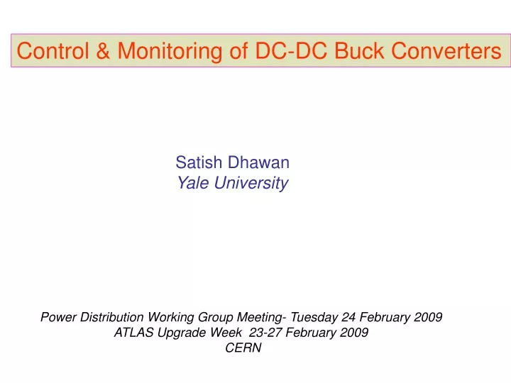
Control & Monitoring of DC-DC Buck Converters. Satish Dhawan Yale University. Power Distribution Working Group Meeting- Tuesday 24 February 2009 ATLAS Upgrade Week 23-27 February 2009 CERN. 3 + 3 Conditions. Do not exceed chip operating voltage.

E N D
Control & Monitoring of DC-DC Buck Converters Satish Dhawan Yale University Power Distribution Working Group Meeting- Tuesday 24 February 2009 ATLAS Upgrade Week 23-27 February 2009 CERN
3 + 3 Conditions • Do not exceed chip operating voltage. • Limit by design the Absolute Maximum output of power supply – Crowbar failure rate 3% • Wire melting protection in case of power shorts • Commercial chips are protected for all normal faults. • Monitor voltages & Temperature & Power Good signal • Soft power on /off (?) Enable PinInductive Kick
Transient kick – with Enb/Dis with power supply Long cables on/off Vmax_Abs = Absolute maximum Vout Vm_op = Maximum Vin operating Inside Buck Regulator Chip Power Supply With Remote Sense Vout On/Off, I, V Enable / Disable Slow Control Power Good / OK Vout Temperature BY DESIGN: Vmax_Abs < Vm_op One Buck per Hybrid = 20 Read out Chips Satish Dhawan Yale University 23 February, 2009 Control & Monitoring of DC-DC Buck Converters
Inside Buck Regulator Chip • Power Down: Low power mode. Shut output switches • Output High side current limit pulse by pulse (turn off high side FET. After 16 times go to soft Start) • Output Low side current limit pulse by pulse (turn off low side FET) • Power OK if Vout with in 10% of set voltage • Vout overvoltage > Disable high side FET • Thermal Shutdown on over temp. Restore on cool down • Good thermal contact to PCB for heat removal • Produce 5V with a LDO from higher voltage • Current monitor 1000:1 Sense FET or 100 mV Resistor shunt • Under voltage Input protection • Slow Turn on but NO SLOW TURN OFF-Inductive Kick ??? Chip Temperature Output is not implemented
From CMS ECAL Powering • LHC 4913 LDO Specifications • maximum operating voltage = 12 volts • Absolute maximum voltage = 14 volts spikes of ~msec • Maximum Vout from Power Supply by Design (and not protection Circuits) =< 12 volts Short Circuit Current Protection • 6.3 Volt 64 Amps Power supplies located 30 meters away. • 4.3 Volts @ 1 to 4 Junction Box • Feed 4 LVR (Low Voltage Regulator Cards – one Trigger Tower). • Maximum Vout from Power Supply by Design (and not protection Circuits) =< 12 volts • Damage to LHC 4913 when power supply output reaches upper rail of 18 /20 volts • 4.3 Volts @ 1 to 4 Junction Box • Feed 4 LVR (Low Voltage Regulator Cards – one Trigger Tower). • Maximum Vout from Power Supply by Design (and not protection Circuits) =< 12 volts
Regulator from Token Ring Link Board
ST Regulator L4913 Data Sheet • Maximum Input Operating Voltage = 12 volts • Absolute Maximum Input Voltage = 14 volts Email explanation from ST Angelo Alberto MESSINA [angelo.messina@st.comWed 6/23/2004 2:47 PM in the ABSOLUTE MAXIMUM RATINGS table in the datasheet we indicate 14V as DC Input Voltage limit. This means that the device can withstand till 14V just for few instants, seconds or even minutes if no further stress are applied; on the contrary 12V is the operative limit. Therefore if the power supply exceeds the output voltage to greater then 14 volts it can damage the regulator for sure. On the other hand in case of 14V sporadic and short spikes the device is internally protected. The question is if your application complies with datasheet recommendations. This because any behavior out of specification, that can occur following the datasheet recommendations, has to be considered as a possible ST failure and has to be managed formally by issuing a F.A.R. (Failure Analysis Request). This F.A.R. has to be request by C.E.R.N. since we need to analyze the damaged parts on a customer report basis. With Over Voltage, ST Regulators can open Circuit >>> Isolating 0.25 µM Electronics OR Short Circuit >>> Damage 0.25 µM Electronics
Distribution Box 0.1 Volt Drop 1 Volt Drop Power Supply GND 4.3 Vanalog 4.3 Vdig + GND GND S+ LVR Board - 11- L4913 S- AWG # 30 wire Inhibit 1.32 mAmps 100 Inhibit Return R13 19.1K 100 R3 10K R19 10 Ώ R14 6.04K 100 DCU Input Gnd 100 Maximum Voltage applied to Inhibit Input = 0.5 V higher then the Power supply Pin (There is a Diode to Vcc Protection in the chip) Inhibit Input Current @ 5 V for one Regulator= 0.12 mAmps For 11 Regulators= 1.32 mAmps A 510 Same as Above 510 B C 510 Same as Above D 510 Inhibit Control Same as Above Locate in or near Power Supply S. Dhawan Yale University 22 February, 2005 LVR Board INHIBIT Control Bits to be changed by CAN Bus Controller in sequential commands. Only one bit to be changed at one time. This is to limit the Ldi/dt voltage spike on turn off