Download
1 / 11
110 likes | 210 Views
Using Contact Probes For Nanomechanical Measurements. Mark R. VanLandingham U. S. Army Research Laboratory Instrumentation and Metrology for Nanotechnology Grand Challenge Workshop January 28, 2004. Outline. Overview of Current Instrumentation Instrumented Indentation Testing (IIT)

E N D
Using Contact Probes For Nanomechanical Measurements Mark R. VanLandingham U. S. Army Research Laboratory Instrumentation and Metrology for Nanotechnology Grand Challenge Workshop January 28, 2004
Outline • Overview of Current Instrumentation • Instrumented Indentation Testing (IIT) • Scanning Probe Microscopy Systems • Atomic force microscope (AFM) • Interfacial force microscope (IFM) • Evolutionary Challenges • Technology-Specific Challenges • General Challenges • Revolutionary Challenges
Indenter Pmax Initial Surface hs a hmax hc Surface Profile at Maximum Force Instrumented Indentation Force Application Device • Variations between different systems include: • How force is applied / measured • How displacement is applied / measured • Feedback control of system • Design for low force capabilities • Device sensitivities • Spring constant • System mass • Quasi-static and dynamic measurement modes • Integrated AFM or AFM-like scanning capabilities Springs Displacement Sensor Springs Probe Tip Sample Load Frame Contact Mechanics
Segmented Photodiode Laser beam Tip Deflection (V) A D C Piezo Scanner B Z-piezo position (nm) Atomic Force Microscope • Tip-sample interaction forces can be measured in force mode • Control vertical motion of cantilever • Tip displacement due to cantilever bending measured by optical lever • Additional steps required to determine indentation response • Probe spring constant can be chosen to optimize force sensitivity. • Combine with contact or tapping mode imaging
Sensor Substrate X-Y-Z Piezo Scanner Capacitor Pads Probe Common Plate Torsion Bars Sample Interfacial Force Microscope • Differential capacitance sensor with force feedback system compliance is zero. • Etched tungsten probes with paraboloidal tips. • Hertzian analysis on loading and/or unloading curves. • SEM profile used to estimate R.
Fused Silica ~100 nm ~100 nm strain Instrumented IndentationChallenges • Large uncertainties at small forces and displacements • Determining point of initial contact • Signal-to-noise issues • Tip shape uncertainties • Reference material calibration • Tip geometry is micrometer scale • Lateral contact dimensions ~ 100 nm for h ~ 13 nm (Berkovich tip) • Significant stress and strain levels extend to depths several times the penetration depth • Use of harmonic oscillation has helped somewhat • Need improved tip manufacturing to move toward the nanoscale • Material independent calibration M Dao, N Chollacoop, KJ Van Vliet, TA Venkatesh, S Suresh, Acta mater. 49 (2001) 3899.
FEA of frictionless contact between probe tip and an infinitely stiff surface before and after probe deflection. Atomic Force MicroscopeChallenges • Address measurement uncertainties • Nonlinearities associated with piezo scanners and photodiode • Probe instabilities • Spring constant uncertainties • Lateral tip motion and/or lateral force caused by bending of the cantilever • Indentation tests are neither displacement nor load controlled • Torsional motion of tip • Non-ideal tip shapes • Use of electrostatic or magnetic force feedback could eliminate many issues • Turn off to image • Additional sensor could be used to measure and control displacement • Improve probe manufacturing techniques • Robust, reproducible, ideal tip shapes
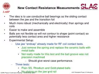
Sensor Substrate X-Y-Z Piezo Scanner Capacitor Pads Probe Common Plate Torsion Bars Sample Interfacial Force MicroscopeChallenges • Problems persist with sensors • Relatively low yield in production • 10% - 70 % depending on part quality • Extremely delicate • Affected by tip mounting and cleaning • Tip manufacturing and mounting issues • Etch tungsten shank to create paraboloidal tip • Tip radius measured using SEM profiles • Tips are adhesively attached to sensor • RF circuitry used with capacitance sensor • Shielding required • Can cause instabilities • Currently developing an interferometric sensor • Suffers from piezo scanner nonlinearities • Use of external sensors to track motion • Imaging capabilities lacking relative to AFM • Software development needed • Ultimately limited by torsion balance vs. cantilever Thanks to Robb Winter for helpful input
Artifacts due to periodicity of spike characterizer Artifact due to joining solutions 300 z (nm) 0 2000 2000 0 y (nm) 0 x (nm) -2000 -2000 35 nm Evolutionary Challenges • Nanoscale tip manufacturing • Tip shape calibration techniques • Revisit needs for tip geometries • Measure more that just E and H • Full stress-strain characterization • Viscoelastic properties of polymers and biomaterials • Mechanical spectroscopy • Increase ranges of frequency space and loading rates • Material-related Issues • Heterogeneity • Tip-sample adhesion • Roughness • High-throughput capabilities • Multi-tip systems MJ Misner, H Skaff, T Emrick, TP Russell, Adv. Mater.15(3) (2003) 221.
Revolutionary Challenges • Combine with other probing techniques • e.g., near-field optical / spectroscopic capabilities • Measure properties as a function of scale • Characterize hierarchical structure from 10-9 m to 10-3 m • Link numerical modeling capabilities into measurement platform • Incorporate material structure, tip geometry, and testing parameters to help analyze data • Material identification through nanomechanical fingerprinting • Access many decades of frequency space • Loading rates from quasi-static to ballistic • Measuring response at the molecular level
Thoughts for Gap Analysis • Nanoscale measurements on hard and soft materials • AFM limited to E ≤ 109 Pa • Does nano, but uncertainty issues KR Shull, Mat. Sci. Eng. R., 36(1)(2002)1. • IIT typically covers 108 Pa to 1012 Pa • Nano is difficult, particularly as E decreases below 1010 Pa • Imaging plus mechanical measurements • SPM cantilevers have unmatched imaging capabilities • Needs much improvement in mechanical measurements • Dual IIT / SPM with nanoscale positioning / registry • Tip shapes • AFM, IFM, and IIT tips all different • Imaging tips vs. mechanical testing tips • AFM tips have non-ideal geometries for mechanical testing • IIT tips not conducive to nanoscale measurements • Lateral force measurement capabilities


![Contact [TC]² for Perfect Body Measurements](https://cdn4.slideserve.com/8150677/contact-tc-for-perfect-body-measurements-dt.jpg)