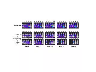
Download
1 / 6
60 likes | 155 Views
Timing Controls. Outline Requirements External Interfaces Schedule Date Needed Prototype Completion Date Hardware Order Date Installation Test Period Design Design Maturity (what reviews have been had) State of Wiring Information State of Prototype. Requirements.

E N D
Timing Controls • Outline • Requirements • External Interfaces • Schedule • Date Needed • Prototype Completion Date • Hardware Order Date • Installation • Test Period • Design • Design Maturity (what reviews have been had) • State of Wiring Information • State of Prototype
Requirements • Timing triggers are sent to devices to synch acquisitions and measurements down the beamline • Triggers are synched to the RF clock • Input timing patterns (PNET SLCNET) arrive at 360 Hz, 1/120 sec in advance of when they are executed • Late updates (during 1/120 sec prior to execution), for eg, MPS status updates, are also accepted • PNET pattern does not include everything. Eg. EPICS timestamp, LCLS MPS rate-limit and mitigation device status must be appended on.
External Interfaces • PNET to LCLS MPG • 128 bit PNET pattern @ 360 Hz including PP, YY, incl/excl mask and a 4 bit countdown to pulse id rollover • LCLS MPG to EVG • 128 bit PNET pattern + EPICS timestamp + LCLS MPS rate limit @ 360 Hz • MPS to LCLS MPG • 16 bit digital input signal containing: • Rate limit: 0, 1, 10, 30, 60, 120, 360 (4 bits) • Rate limit origin:number of 360 Hz pulses before the new rate limit will begin (7 bits) • Portion of pulse id: for comparison (2 bits) • Mitigation device(s) in place: none, Pockel’s cell, single bunch beam dumper, both(2 bits) • EVG to EVG fanout to EVRs • EVG sends LCLS MPG data (above) to EVRs at 360 Hz via an EVG fanout module • EVRs to EVR transition modules • EVRs send triggers out after once timer counting programmed delay is done • EVR transition modules to devices • Trigger signals data acquisition and measurement
Schedule • Date Needed: to BC1: Dec/06 • Prototype Completion Date: VME: Mar/06 PMC: Jul/06 • Hardware Order Date:Apr/06 • Hardware Delivery Date:Jun/06 • Installation in injector: Oct/06 • Test Period: Nov/06
Design • Design maturity (what reviews have been had): • EPICS Collaboration Meeting Timing Session • Establishing collaboration between LANL, ORNL, KEK and SLAC for next generation timing system • PNET Design Review 19May2005 • Timing presentation at Lehman Review, May 10-12, 2005 • Timing SCR/PDR by controls group, Nov 16-17, 2005 Docs at: http://www.slac.stanford.edu/grp/lcls/controls/global/subsystems/timing/ • State of wiring: percent complete Captar input will be given at time of presentation • State of prototype: PNET part done. EVG/VME EVR 200 in house. Converting driver and device support to RTEMS