Download
1 / 20
510 likes | 1.52k Views
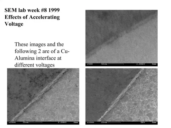
Effect of Accelerating Voltage on SEM Resolution. Hong Koh Yiin -CAMTEC 2011-. Image from: http://www.sciencephoto.com/media/99504/enlarge. Accelerating Voltage. Voltage difference between the filament (cathode) and the anode Accelerates the electron beam towards the anode. . Resolution.

E N D
Effect of Accelerating Voltage on SEM Resolution Hong KohYiin -CAMTEC 2011- Image from: http://www.sciencephoto.com/media/99504/enlarge
Accelerating Voltage • Voltage difference between the filament (cathode) and the anode • Accelerates the electron beam towards the anode.
Resolution • The minimum distance that can be separated as two distinguishable points in the SEM image. SEM Resolution Test Medium (Al-W Dendrites)
Relationship between the Accelerating Voltage and the Resolution Primary electron beam Secondary electrons 2 1 Resolution (nm) Backscattered electrons FE-SEM (S-4800) X-rays 1 15 Accelerating Voltage (kV)
Secondary electron emission signal – more widely used in SEM Secondary Electron Detector
Relationship Between Electrons and Accelerating Voltage Energy of accelerated electron, E = eV = ½ mv2 e = charge of electron V = accelerating voltage m = rest mass of electron v = velocity of electron http://www.microscopy.ethz.ch/properties.htm
http://www.ammrf.org.au/myscope/sem/practice/principles/voltagevstype.phphttp://www.ammrf.org.au/myscope/sem/practice/principles/voltagevstype.php
Penetration Depth, H = 0.0276 A V 1.67 , μm z0.89 ρ A= atomic weight, g mol-1 V= accelerating voltage, kV z= atomic number ρ= density, g cm-3 Penetration Depth α Interaction Volume
Penetration Depth in Different Accelerating Voltage SrS 5000Å Si • Penetration depth/interaction volume is a direct function of energy. 15 kV 10 kV 5 kV
High Unclear surface structures More edge effect High Resolution More charge-up More beam damage Accelerating Voltage Clear surface structures Low Resolution Less edge effect Less charge-up Less beam damage Low
Unclear surface structures High More edge effect High Resolution More charge-up More beam damage Accelerating Voltage Clear surface structures Low Resolution Less edge effect Less charge-up Less beam damage Low
Unclear surface structures High More edge effect High Resolution More charge-up More beam damage Accelerating Voltage Clear surface structures Low Resolution Less edge effect Less charge-up Less beam damage Low
Unclear surface structures High More edge effect High Resolution More charge-up More beam damage Accelerating Voltage Clear surface structures Low Resolution Less edge effect Less charge-up Less beam damage Low
200nm 5 kV, 50000x 2 kV, 50000x 300 V, 50000x 200nm