Download
1 / 26
270 likes | 294 Views
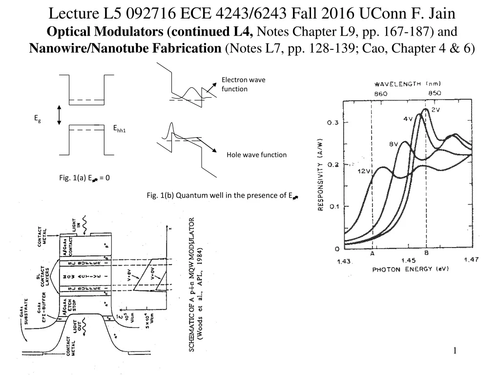
Lecture L5 092716 ECE 4243/6243 Fall 2016 UConn F. Jain Optical Modulators (continued L4, Notes Chapter L9, pp. 167-187) and Nanowire / Nanotube Fabrication (Notes L7, pp. 128-139; Cao, Chapter 4 & 6). Electron wave function. E g. E hh1. Hole wave function. Fig. 1(a) E = 0.

E N D
Lecture L5 092716 ECE 4243/6243 Fall 2016 UConn F. Jain Optical Modulators (continued L4, Notes Chapter L9, pp. 167-187) and Nanowire/Nanotube Fabrication (Notes L7, pp. 128-139; Cao, Chapter 4 & 6) Electron wave function Eg Ehh1 Hole wave function Fig. 1(a) E = 0 Fig. 1(b) Quantum well in the presence of E Ee1
Phase Modulator: A light beam signal (pulse) undergoes a phase change as it transfers an electro-optic medium of length ‘L’ Change in index of refraction ------------- (1) In linear electro-optic medium …………………(2) E= Electric field of the RF driver; E=V/d, V=voltage and d thickness of the layer. r= linear electro-optic coefficient n= index
Figure compares linear and quadratic variation Dn as a funciton of field. MQWs have quadratic electro-refractive effect. Figure shows a Fabry-Perot Cavity which comprises of MQWs whose index can be tuned (Dn) as a funciton of field.
Mach-Zehnder Modulator Here an optical beam is split into two using a Y-junction or a 3dB coupler. The two equal beams having ½ Iin optical power. If one of the beam undergoes a phase change , and subsequently recombine. The output Io is related as Mach-Zehnder Modulator comprises of two waveguides which are fed by one common source at the input (left side). When the phase shift is 180, the out put is zero. Hence, the applied RF voltage across the waveguide modulates the input light.
Heterostructure Acoustic Charge Transprot HACT Modulator (pp. 187-192)
Electro-Optic, Acousto-Optic Modulators (pp. 193-197) Electro-Optic, Acousto-Optic Modulators (pp. 193-197)
Nanowire Fabrication (Notes L7 p. 128) Synthesis: • Nanowires using supersaturated semiconductor-gold alloys in vapor phase • Nanotubes: (a) carbon nanotubes (b) SiC and other non-carbon nanotubes • Quantum dots using chemical synthesis from liquid or vapor phase. Etching: Thin quantum well epitaxial layers are grown in appropriate device structure, in–plane etching using nanolithographic techniques. Reactive ion etching, ion milling are two commonly used etching techniques. Lithography • Imersion lithography using 193 nm Excimer laser • Extreme Ultra Violet (EUV) • 13.5 nm • Sn Plasma. 35 Mw • Xe ASML (Wilton, CT) and Nanotech. Albany
Nanowire Fabrication (Cao, Chapter 4, pp. 129-130) Growth of Si nanowires using VLS technique
Nanowire Fabrication (Cao, Chapter 4, pp. 132-133) Comparison of axial and lateral Growth of Si and Ge nanowires using VLS technique
Nanowire Fabrication (Cao, Chapter 4, pp. 141) Comparison of Growth using VLS and SLS techniques
Nanowire Fabrication (Cao, Chapter 4, pp. 153) Electrophoresis and Electro-spinning
Nanowire Fabrication (Cao, Chapter 4, pp. 165) Electrophoresis and Electro-spinning
Single-Walled Carbon Nanotube Gated FET • Self-Assembly Methodology • I-V Characteristics • Functionalization Methods Croce et. Al., Sensorsand Actuators B: Chemical, Vol. 160, 1, pp. 154-160, 2011 [1] Device W/L = 100mm/30mm
Methodologies for CNT FET Based-Bio/Chemical Sensing CNT Channel FETs (Previous Work) CNT Gate FETs (Our work) Croce et al. [1] Cid et al. [9] Abe et al. [10]
CNT Self-Assembly Scheme on the Gate Region of the MOSFET Croce et. al., Sensorsand Actuators B: Chemical, Vol. 160, 1, pp. 154-160, 2011 [1]
Control CNT Gate FET, no DNA/Thrombin Cross-Sectional Device Schematic ID-VD Device Characteristics 12/19/2019
CNT liquid gate FET: Results • Functionalization 50 µM Thrombin, wash in .1% SDS • Addition of Thrombin in PBS to Gate, .1, .7 , 1 µM • Gate voltage applied through platinum electrode
CNT Liquid Gate FET: Analysis (a) Energy band diagram with ssDNA aptamer functionalization and the addition of thrombin. (b) Charge density diagram of the ssDNA functionalized SWNT device and (c) with the addition of thrombin. 12/19/2019
Aptamer Functionalization Scheme on CNTs Assembled on the Gate • ssDNA Thrombin Aptamer (5’-GGTTGGTGTGGTTGG-3’) modified on 3’ end with NH2