Download
1 / 4
40 likes | 207 Views
Impact on High-Performance Applications: FPGA Chip Bandwidth at 40 nm. J. Ryan Kenny Altera Corporation 101 Innovation Drive San Jose, CA 95134. High-Performance Embedded Computing Workshop 23-25 September 2008. 40-nm Transceiver Eye and Jitter Test Set Up.

E N D
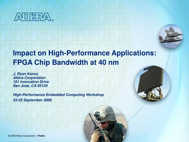
Impact on High-Performance Applications: FPGA Chip Bandwidth at 40 nm J. Ryan Kenny Altera Corporation 101 Innovation Drive San Jose, CA 95134 High-Performance Embedded Computing Workshop 23-25 September 2008
40-nm Transceiver Eye Diagram at 8.5 and 10 Gbps 8.5 Gbps 10 Gbps 8.5 Gbps 10 Gbps Pattern VOD DJ RJ (RMS) RJ (RMS) PRBS 7 600 mV 10.3 ps 1.23 ps 1.35 ps Extraordinary jitter performance
High-Performance Applications • In excess of 100 Gbps • (Mixture of 8.5 Gbps and 3.125 Gbps) Soon: Drive optical Chip-to-chipbandwidth Chip-to-backplane • As many as 48 lanes • 24 up to 8.5 Gbps • 10G optical • (Future)