Download
1 / 8
80 likes | 166 Views
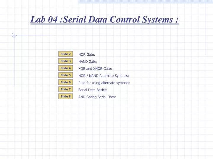
Lab 04 :Serial Data Control Systems :. Slide 2. NOR Gate:. Slide 3. NAND Gate:. Slide 4. XOR and XNOR Gate:. Slide 5. NOR / NAND Alternate Symbols:. Slide 6. Rule for using alternate symbols:. Slide 7. Serial Data Basics:. Slide 8. AND Gating Serial Data:. Logic 1. Logic 1.

E N D
Lab 04 :Serial Data Control Systems : Slide 2 NOR Gate: Slide 3 NAND Gate: Slide 4 XOR and XNOR Gate: Slide 5 NOR / NAND Alternate Symbols: Slide 6 Rule for using alternate symbols: Slide 7 Serial Data Basics: Slide 8 AND Gating Serial Data:
Logic 1 Logic 1 Logic 0 Logic 0 Logic 0 Logic 0 Logic 0 Logic 1 5v NOR Logic 0 5v Input A Logic 1 Output X Logic 1 Logic 0 Input B 5v Lab 04 : NOR Gate The NOR gate is equivalent to an OR gate with a NOT gate connected to its output. NOR comes from the words Not OR. Continue to see the standard symbol for NOR. NOR Symbol Truth Table: The table shows that the NOR gate responds with a low at the output if the signal applied to the input A or B is high. System animation: In order to see how it works, the gate has been connected to 2 switches and LED. Continue to see the system in action… Boolean Equation: here is the equation for the NOR gate. Slide #2
Logic 1 Logic 1 Logic 0 Logic 0 Logic 0 Logic 1 Logic 1 5v Logic 1 NAND 5v Input A Logic 1 Logic 0 Output X Logic 0 Logic 1 Input B 5v Lab 04 : NAND Gate The NAND gate is equivalent to an AND gate with a NOT gate connected to its output. NAND comes from the words Not AND. Continue to see the standard symbol for NAND. NAND Symbol Truth Table: The table shows that the NAND gate responds with a low at the output if the signal applied to the input A and B is high. System animation: In order to see how it works, the gate has been connected to 2 switches and LED. Continue to see the system in action… Boolean Equation: here is the equation for the NAND gate. Slide #3
XOR XNOR Input A Input A Output X Output X Input B Input B Lab 04 : XOR Gate The XOR gate is an exclusive OR gate. It will output a logic 1 if there is an exclusive logic 1 at input A or B. Exclusive means: Only one input can be high at one time. Truth Table: The table shows that the XOR gate responds with a high at the output if the signal applied to the input A or B is high (but not both high). XOR Boolean Equation: The XNOR gate is an exclusive OR gate with an NOT gate at the output. It will output a logic 0 if there is an exclusive logic 1 at input A or B. XOR Boolean Equation: Slide #4
NOT NOR NAND 0 OR 0 = 1 0 AND 0 = 1 Alternate NOR Alternate NAND Lab 04 : NOR and NAND Gate Alternate Symbols: The NAND and NOR logic gate symbols you have studied are called the “standard” symbols. Each gate also has an “alternate” symbol. The “standard” logic symbols for the NAND and NOR gates indicates a gates response to “logic 1” at the input. Alternate NOR GATE: The bubbles at the input of the NOR gate implies that a “logic 0” at input A and a “logic 0” at input B are required to produce a “logic 1” at output X (NO bubble at output). Alternate NAND GATE: The bubbles at the input of the NAND gate implies that a “logic 0” at input A or a “logic 0” at input B are required to produce a “logic 1” at output X (NO bubble at output). Slide #5
= = = 5V Active High LED Active Low LED A logic 1 lights the LED 1 A logic 0 lights the LED 0 Lab 04 :Rule for Using the Alternate symbols : The basic logic gates AND, OR, and NOT have standard logic symbols and alternate logic symbols. A general rule for using alternate symbols exists. The rule is a guide and not a strict rule. Some designers do not use the rule but many do. Standard Alternate The rule is simple : Active high device connects to active high symbol : Active low device connects to the active low symbol. Example: Connect an LED to an AND gate: There are two types of LED connections. Active high device connects to active high symbol (standard).Active low device connects to the active low symbol (alternate). Slide #6
1 0 2- The inverse of the Serial Data is transferred. Y = B The series of 1’s and 0’s can sent to a device like a printer. The printer can group the bits into a code. The code could be used to print out a character on a piece of paper. A 5v 5v Control Switch A Y 1 Logic Gate B 0 1- The Serial Data is transferred. Y=B 1 1 0 0 4- The Serial Data is blocked. Output Y= Logic 1. 3- The Serial Data is blocked. Output Y= Logic 0. 1 1 0 0 0 0 1 1 1 1 1 1 0 0 1 1 0 0 Lab 04 : Gating digital signals: Basic Theory Digital systems communicate to each other using a Serial Data stream. You will learn what Serial Data is and how logic gates can be used to control the flow of this digital information. Serial Data is a pulse waveform The pulse waveform represents a series of 1’s and 0’s. A Logic Gate and a Control Switch can be used to build a control system. This system can alter the transfer of Serial Data from input B to output Y. The position of the Control Switch (1 or 0) and the type of Logic Gate (AND, OR, NOR …) create different control schemes. However all control schemes generate responses from a group of 4: Slide #7
AND Gate 5v 5v B Control Switch 1 0 0 1 1 1 0 0 1 1 0 A Y A B The next section B=0 and A=1. For an AND gate the response is Y=0. Draw Y for that section. The next section B=0 and A=0. For an AND gate the response is Y=0. Draw Y for that section. The next section B=1 and A=1. For an AND gate the response is Y=1. Draw Y for that section. Start at the the first section B=1 and A=0. For an AND gate the response is Y=0. Draw Y for that section. Lab 04 : AND Gating digital signals The “And Gate” will be used to control the flow of Serial Data. Waveforms will be drawn to determine the output response (Y). The position of the Control Switch is represented by waveform A. When A=0 the switch is in the lower position. When A=1 the switch is in the upper position. Proceed to view the animation. To draw the output response (Y) it is helpful to draw vertical lines at each transition of waveform A and B. The vertical lines create horizontal sections. These sections will be used to determine the output response. Continue to use this technique to complete the drawing of output waveform Y. Now that the waveform is drawn we can proceed to a more general discussion about the control system. Y The AND gate blocks the Serial Data and Y=0 when the Control Switch is 0. The AND gate passes the Serial Data and Y=B when the Control Switch is 1. Slide #8