Download
1 / 42
470 likes | 568 Views
Crystal Structure and Polysilicon Preparation. Dr. S. K. Bhatnagar Professor and Head, R & D Center for Engg. And Science, J. E. C. Kukas. www.studygalaxy.com. Raw material - silicon. Silicon wafers are required for IC manufacturing, These should meet certain specifications,

E N D
Crystal StructureandPolysilicon Preparation Dr. S. K. Bhatnagar Professor and Head, R & D Center for Engg. And Science, J. E. C. Kukas www.studygalaxy.com
Raw material - silicon Silicon wafers are required for IC manufacturing, These should meet certain specifications, Silicon ingots are needed to produce these wafers, How these ingots are produced? How silicon is produced to manufacture these ingots? What is the desired structure of the silicon?
Structures of Solid Materials S. K. Bhatnagar (August 2010)
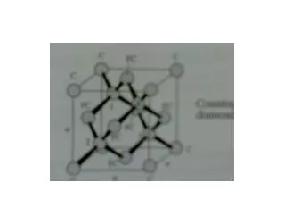
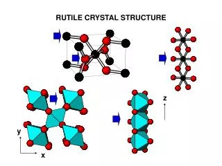
Crystal Structure • A crystal structure is a unique arrangement of atoms in a crystal. • Lattice is an array of points repeating periodically in three dimensions. • The points can be thought of as forming identical tiny boxes, called unit cells, that fill the space of the lattice. • The lengths of the edges of a unit cell and the angles between them are called the lattice parameters. S. K. Bhatnagar (August 2010)
Miller Indices • Miller indices are a notation system in crystallography for planes and directions in crystal lattices. S. K. Bhatnagar (August 2010)
Defects in Crystals • What is a DEFECT? • Any imperfaction in the crystal is called a defect • Categories of defects: 4 types depending on their dimensionality • Point Defect • Dislocation (line defect) • Area or Planar Defect • Volume Defect S. K. Bhatnagar (August 2010)
Simple defects in crystals S. K. Bhatnagar (August 2010)
Point Defect S. K. Bhatnagar (August 2010)
Dislocation S. K. Bhatnagar (August 2010)
When a defect is spread over an area it is called an ‘Area Defect’. Examples: Twin Boundary Grain Boundary Area (Planar ) Defect S. K. Bhatnagar (August 2010)
When a defect is spread over a volume it is called a ‘Volume Defect’ Example: Precipitates of impurity (dopants) Volume Defect S. K. Bhatnagar (August 2010)
Charged Defects • Vacancies may be charged also • Charge interaction in a solid = chemical reactions in solutions, • Concentration of vacancies determined by Mass-action relationships, • Impurity conc. Gradient electric field in semiconductors • Conc. Of neutral vacancies unaffected by this electric field. Hence, this conc. is same in extrinsic and intrinsic semiconductors S. K. Bhatnagar
Conc. Of neutral vacancies fn of Temperature • Conc. Of charged vacancies fn of Temp. and Impurity Conc. (due to E field) • Hence Total Vacancy conc. fn of Impurity conc. • Reactions involved: • Vo + h+ ↔ V+ • Vo + e- ↔ V- • Vo + 2e- ↔ V2- • Charged vacancies have self compensating effect on the semiconductor • P-type material will have V+ which is donor- like • N-type material will have V- which is acceptor-like S. K. Bhatnagar (September 2010)
Solid Solubility • Solid solubility is the conc. Of the impurity that the host lattice can accept in a solid solution of itself and impurity, • Retrograde solubility: • Solubility decreases with decreasing temp. • Effect: Precipitation of impurity at lower temp. generation of volume defects S. K. Bhatnagar
How? • Maximum conc. At high temp • Cool down the crystal, lower solid solubility at lower temp. • So the solution is supersaturated • To achieve equilibrium impurity atoms in excess of solid solubility (at lower temp.) are precipitated as a second phase. (silicides) • Precipitates undesirable sites of dislocation generation, S. K. Bhatnagar (September 2010)
Gettering (S. M. SZE p.45) • What is Gettering? • A process that removes harmful impurities or defects from the regions in a wafer where devices are fabricated, • Advantages: • Improvements in junction leakage current • How it is done? • Trapping sites are intentionally created to trap the harmful impurities so that they become immobile • Bulk of the wafer does not participate in device functioning. Therefore traps are introduced on the back surface of the wafer, S. K. Bhatnagar
Gettering Techniques (S. M. SZE p.45) • Pre-Gettering: • Gettering before device fabrication provides sinks that absorb impurities during device fab. • Back surface damaging done intentionally • Mechanically lapping, sand blasting • By LASER beam • Thermal Treatments at different temps. S. K. Bhatnagar
Gettering Techniques (S. M. SZE p.45) • Intrinsic Gettering: • Oxygen present in the wafer is precipitated to provide trapping sites, • High Temperature Cycle (>1050 o C in N2) to evaporate Oxygen from near the wafer surface, • Thus supersaturation condition near the surface is avoided. A defect free zone is obtained for device fab. This zone is called Denuded Zone • Low temperature treatment to precipitate oxygen in the bulk, S. K. Bhatnagar
Gettering Techniques (S. M. SZE p.45) • Metallic Gettering; • A metal e.g. Nickel evaporated on the ack surface of wafer. • Heat treatment for adhesion, • Impurities e.g. gold having higher solubility in Nickel get trapped in it. • Polysilicon Gettering: • Deposit 1 micron thick polysilicon on the back surface • Grain boundaries in poly act as traps for impurities S. K. Bhatnagar (September 2010)
Purification of materials:Purpose: • Chemically reduce the material – if it is an oxide, • Convert it in a form (solid, liquid or gas) so that it can be separated from other materials, • What is distillation? • Why we do it? • Fractional distillation? S. K. Bhatnagar (August 2010)
MGS and EGS • What is MGS? • Metallurgical processes are used to produce Silicon from its ore. • SiO2 + C Si + 2 CO (reduction of oxide under heat and electric field) • Result MGS • What is EGS? • Chemical purification of MGS • Convert Si in a volatile compound to separate it from impurities • Si + 3HCl SiHCl3 + H2 • Convert TCS back into Si The resultant product is highly pure Si called EGS S. K. Bhatnagar (August 2010)
Crude Silicon and its purification:Process Steps: heat • SiO2+ 2 C Si + 2 CO sand coal Metallurgical grade (MGS) heat(300 C) • Si + 3 HCl SiHCl3 + H2 MGS TCS heat (1100 C) • SiHCl3 + H2 Si + 3 HCl TCS EGS S. K. Bhatnagar (August 2010)
From Silicon to Trichlorosilane (TCS):* Purpose:* Process Steps: Si + HCl TCS S. K. Bhatnagar (August 2010)
From TCS to Electronic Grade Silicon (EGS):* Purpose:* Process Steps: S. K. Bhatnagar (August 2010)
Crystal Growing Theory • Every impurity has a solid solubility in Silicon and a different equilibrium solubility in the melt. • Segregation Coefficient k0 = Cs / Cl • Cs , Cl = equilibrium concentrations of the impurity in the solid and melt near the interface S. K. Bhatnagar (August 2010)
Unit – 1: Introduction to technologies • Syllabus: • Semiconductor Substrate-Crystal defects, Electronic Grade Silicon, • Czochralski Growth, Float Zone Growth, • Characterization & evaluation of Crystals; • Wafer Preparation- Silicon Shaping, Etching and Polishing, Chemical cleaning. S. K. Bhatnagar (August 2010)
Plan of Lecture • Crystal Structure and Crystal Defects • Preparation of polycrystalline silicon • Crystal Growing Theory • Preparation of single crystal silicon • Wafer Preparation S. K. Bhatnagar (August 2010)
Mono-crystal Silicon Growth • Crystal Pulling • CZ Method • Floating Zone Method S. K. Bhatnagar (August 2010)
Czochralski (CZ)crystal growth It involves the crystalline solidification of atoms from a liquid phase at an interface. The process consists of the following steps: A fused silica crucible is loaded with a charge of undoped EGS together with a precise amount of diluted silicon alloy. Evacuate the growth chamber. Back-fill with inert gas prevent atmospheric gases from entering the chamber. S. K. Bhatnagar (August 2010)
Czochralski (CZ)crystal growth • Heat Crucible to 1421o C to melt Silicon. • Introduce seed crystal in molten silicon. Seed crystal is slim ( 5 mm dia) and 100 – 300 mm long with precise orientation • The seed crystal is then withdrawn at a very controlled rate. • The seed crystal and the crucible are rotated in opposite directions while this withdrawal process occurs. S. K. Bhatnagar (August 2010)
h103 S. K. Bhatnagar (August 2010)
q410 S. K. Bhatnagar (August 2010)
h104 S. K. Bhatnagar (August 2010)
q421 S. K. Bhatnagar (August 2010)
q411 S. K. Bhatnagar (August 2010)
Crystal Structure • A crystal structure is a unique arrangement of atoms in a crystal. • It is composed of motifs and a lattice. • Motif is a set of atoms arranged in a particular way. • Lattice is an array of points repeating periodically in three dimensions. S. K. Bhatnagar (August 2010)
Crystal Structure (contd.) S. K. Bhatnagar (August 2010) Motifs are located upon the points of a lattice. The points can be thought of as forming identical tiny boxes, called unit cells, that fill the space of the lattice. The lengths of the edges of a unit cell and the angles between them are called the lattice parameters.