Download
1 / 28
280 likes | 426 Views
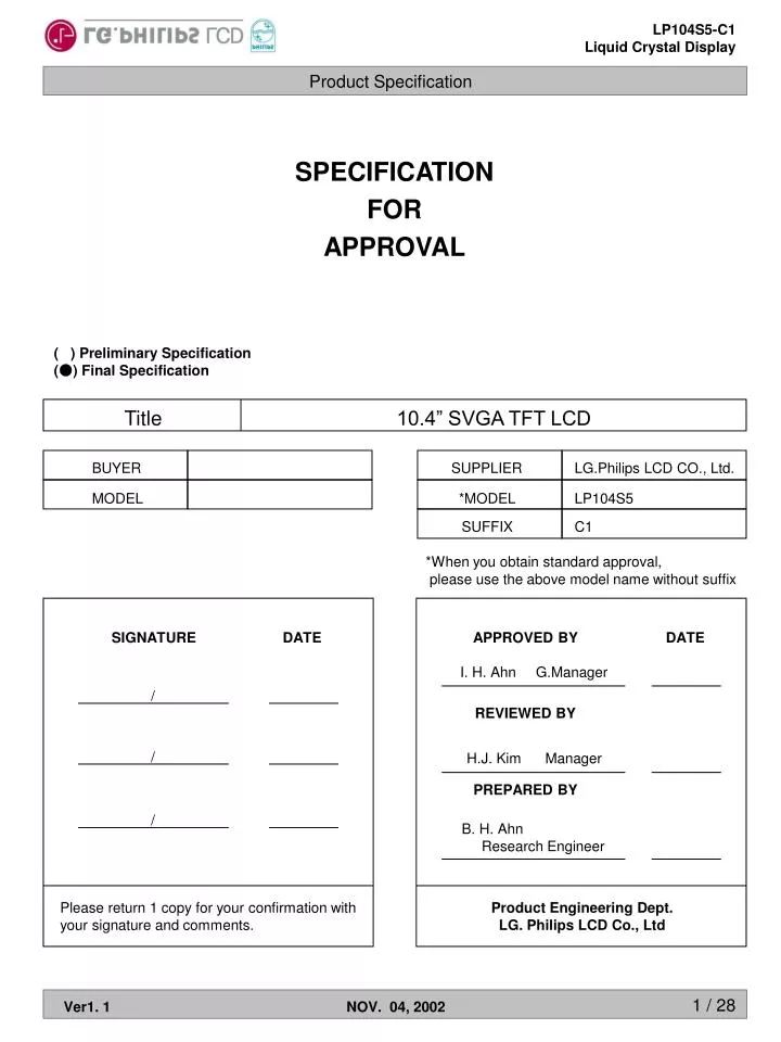
SPECIFICATION FOR APPROVAL. ( ) Preliminary Specification (●) Final Specification. Title. 10.4” SVGA TFT LCD. BUYER. SUPPLIER. LG.Philips LCD CO., Ltd. MODEL. *MODEL. LP104S5. SUFFIX. C1. *When you obtain standard approval, please use the above model name without suffix.

E N D
SPECIFICATION FOR APPROVAL ( ) Preliminary Specification (●) Final Specification Title 10.4” SVGA TFT LCD BUYER SUPPLIER LG.Philips LCD CO., Ltd. MODEL *MODEL LP104S5 SUFFIX C1 *When you obtain standard approval, please use the above model name without suffix SIGNATURE DATE APPROVED BY DATE I. H. Ahn G.Manager / REVIEWED BY / H.J. Kim Manager PREPARED BY / B. H. Ahn Research Engineer Please return 1 copy for your confirmation with your signature and comments. Product Engineering Dept. LG. Philips LCD Co., Ltd
NO. ITEM Page - 1 COVER - CONTENTS 2 - 3 RECORD OF REVISIONS GENERAL DESCRIPTION 1 4 ABSOLUTE MAXIMUM RATINGS 5 2 6 3 ELECTRICAL SPECIFICATIONS 6 3-1 ELECTRICAL CHARACTREISTICS 8 3-2 INTERFACE CONNECTIONS 3-3 SIGNAL TIMING SPECIFICATIONS 9 3-4 10 SIGNAL TIMING WAVEFORMS COLOR INPUT DATA REFERNECE 11 3-5 POWER SEQUENCE 12 3-6 4 OPTICAL SPECIFICATIONS 13 5 MECHANICAL CHARACTERISTICS 17 RELIABILITY 21 6 INTERNATIONAL STANDARDS 7 22 22 7-1 SAFETY 22 EMC 7-2 8 PACKING 23 DESIGNATION OF LOT MARK 23 8-1 23 8-2 PAKING FORM 9 24 PRECAUTIONS
Revision No Revision No Page DESCRIPTION 1.0 1.1 SEP 29, 2002 NOV 04,2002 - 14Page 15Page ● First Draft ●Color change due to CF change ● Modified a gamma value RECORDS OF REVISIONS
1. General Description The LP104S5-C1 is a Color Active Matrix Liquid Crystal Display with an integral Cold Cathode Fluorescent Lamp(CCFL) backlight system. The matrix employs a-Si Thin Film Transistor as the active element. It is a transmissive type display operating in the normally white mode. This TFT-LCD has 10.4 inches diagonally measured active display area with SVGA resolution(600 vertical by 800 horizontal pixel array) Each pixel is divided into Red, Green and Blue sub-pixels or dots which are arranged in vertical stripes. Gray scale or the brightness of the sub-pixel color is determined with a 6-bit gray scale signal for each dot, thus, presenting a palette of more than 262,144 colors. The LP104S5-C1 has been designed to apply the interface method that enables low power, high speed, low EMI. Flat Link must be used as a LVDS(Low Voltage Differential Signaling) chip. The LP104S5-C1 is intended to support applications where thin thickness, low power are critical factors and graphic display are important. In combination with the vertical arrangement of the sub-pixels, the LP104S5-C1 characteristics provide an excellent flat display for office automation products such as Mini-Notebook PC or Web-pad, etc. Timing Column driver circuit Control Block CN1 Flat Link interface TFT - LCD Row Driver circuit ( 800 X 600) Power Block CN Backlight Ass’y 2 CN1: DF19K - 20P - 1H or equivalent , CN2: BHSR - 02VS - 1 (JST) General Features Active screen size 10.4 inches (264.16mm) diagonal Outline Dimension 224.5(H) x 172.0(V) x 5.7(D) mm(Typ.) Pixel Pitch 0.264 mm x 0.264mm Pixel format 800 horiz. By 600 vert. Pixels RGB stripes arrangement Color depth 6-bit, 262,144 colors Luminance, white 220 cd/m2(Typ.) Power Consumption Total 4 Watt(Typ.) Weight 295g(Typ.) Display operating mode Transmissive mode, normally white Hard coating(3H) Anti-glare treatment of the front polarizer, HAZE(13%) Surface treatments
Values Parameter symbol Units Notes Min. Max. At 25 5°C 1 1 1 1 Power Input Voltage Operating Temperature Storage Temperature Operating Ambient Humidity Storage Humidity VCC TOP TST HOP HST -0.3 0 -20 10 10 4.0 50 60 90 90 Vdc °C °C %RH %RH 90% 80% 60% 60 Wet Bulb Temperature [℃] 50 Humidity[(%)RH] Storage 40% 40 30 Operation 20 20% 10 0 10% -20 0 10 60 70 80 20 30 40 50 Dry Bulb Temperature [℃] 2. Absolute Maximum Ratings The following are maximum values which, if exceeded, may cause faulty operation or damage to the unit. Table 1. ABSOLUTE MAXIMUM RATINGS Note : 1. Temperature and relative humidity range are shown in the figure below. Wet bulb temperature should be 39 °C Max, and no condensation of water.
Values Parameter Symbol Units Notes Min. Typ. Max. VCC ICC Zm PC 3.0 - 90 - 3.3 303 100 1.0 3.6 340 110 1.1 Vdc mA ohm Watts 1 2 1 MODULE : Power Supply Input Voltage Power Supply Input Current Differential Impedance Power Consumption VBL IBL VS f BL Ts PBL LAMP : Operating Voltage Operating Current Established Starting Voltage at 25 °C at 0 °C Operating Frequency Discharge Stabilization Time Power Consumption Life Time 485 3.0 - - 45 - 20,000 500 6.0 - - 60 3.0 - 600 6.5 845 1015 80 3 3.3 - VRMS mA VRMS VRMS kHz Minutes Watts Hrs 3 4 5 6 7 8 3. Electrical Specifications 3-1. Electrical Characteristics The LP104S5-C1 requires two power inputs. One is employed to power the LCD electronics and to drive the TFT array and liquid crystal. The second input which powers the CCFL, is typically generated by an inverter. The inverter is an external unit to the LCD. Table 2. ELECTRICAL CHARACTERISTICS Note : The design of the inverter must have specification for the lamp in LCD Assembly. The performance of the Lamp in LCM, for example life time or brightness, is extremely influenced by the characteristics of the DC-AC inverter. So all the parameters of an inverter should be carefully designed so as not to produce too much leakage current from high-voltage output of the inverter. When you design or order the inverter, please make sure unwanted lighting caused by the mismatch of the lamp and the inverter(no lighting, flicker, etc) never occurs. When you confirm it, the LCD Assembly should be operated in the same condition as installed in you instrument. 1. The specified current and power consumption are under the VCC=3.3V, 25°C,fV=60Hz condition whereas mosaic pattern is displayed and fV is the frame frequency. 2. This impedance value is needed to proper display and measured from LVDS TX to the mating connector. 3. The variance of the voltage is 10%. 4. The voltage above VS should be applied to the lamps for more than 1 second for start-up. Otherwise, the lamps may not be turned on. The used lamp current is the lamp typical current.
5. The output of the inverter must have symmetrical(negative and positive) voltage waveform and symmetrical current waveform.(Unsymmetrical ratio is less than 10%) Please do not use the inverter which has unsymmetrical voltage and unsymmetrical current and spike wave. Lamp frequency may produce interface with horizontal synchronous frequency and as a result this may cause beat on the display. Therefore lamp frequency shall be as away possible from the horizontal synchronous frequency and from its harmonics in order to prevent interference. 6. Let’s define the brightness of the lamp after being lighted for 5 minutes as 100%. Ts is the time required for the brightness of the center of the lamp to be not less than 95%. 7. The lamp power consumption shown above does not include loss of external inverter. The used lamp current is the lamp typical current. 8. The life is determined as the time at which brightness of the lamp is 50% compared to that of initial value at the typical lamp current on condition of continuous operating at 25 2°C. 9. Do not attach a conducting tape to lamp connecting wire. If the lamp wire attach to a conducting tape, TFT-LCD Module has a low luminance and the inverter has abnormal action. Because leakage current is occurred between lamp wire and conducting tape.
3-2. Interface Connections Interface chip must be used FlatLink, part No. THC63LVDM63A(Transmitter), THC63LVDF64A(Receiver) made by Thine Microsystems, Inc. This LCD employs two interface connections, a 20 pin connector is used for the module electronics and the other connector is used for the integral backlight system. The electronics interface connector is a model DF19K-20P-1H manufactured by HIROSE. The pin configuration for the connector is shown in the table below. Table 3. MODULE CONNECTOR PIN CONFIGURATION(LVDS) Pin Symbol Description Notes 1 2 3 4 5 6 7 8 9 10 11 12 13 14 15 16 17 18 19 20 Vcc Vcc GND GND A1M A1P GND A2M A2P GND A3MA3P GND CLKM CLKP GND GND GND GND GND Power(3.3V) Power(3.3V) Ground Ground Differential Signal Differential Signal Ground Differential Signal Differential Signal Ground Differential Signal Differential Signal Ground Differential Signal Differential Signal Ground No Connection No Connection Ground Ground 1. Interface chips 1.1 LCD : LPZ4E102S6L (KZ4E028F14) including LVDS Receiver 1.2 System : THC63LVDM63A or Equivalent *Pin to Pin compatible with TI LVDS 2. Connector 2.1 LCD : DF19K-20P-1H (HIROSE) 2.2 Mating : Discrete Wire type : DF19G-20S-1C (HIROSE) FPC type : DF19G-20S-1F (HIROSE) 2.3 Connector pin arrangement 1 20 Source PCB ▶ [LCD Module rear view] * Refer to page 20 to get details The backlight interface connector is a model BHSR-02VS-1, manufactured by JST. The mating connector part number is SM02B-BHSS-1 by JST or equivalent. The pin configuration for the connector is shown in the table below. Table 4. BACKLIGHT CONNECTOR PIN CONFIGURATION Pin Symbol Description Notes 1 2 HV LV 1 1 Power supply for lamp (High voltage side) Power supply for lamp (Low voltage side) Notes : 1. The high voltage side terminal is colored pink. The low voltage side terminal is black.
Table 5. REQUIRED SIGNAL ASSIGNMENT FOR FlatLink Transmitter Notes : Refer to LVDS Transmitter Data Sheet for detail descriptions.
3-3. Signal Timing Specifications This is the signal timing required at the input of the LVDS Transmitter. All of the interface signal timing should be satisfied with the following specifications for it’s proper operation. Table 6. Timing Table
0.7Vcc Hsync, Vsync, DE, DATA 0.3Vcc tCLK 0.5VCC Dclk VALID INVALID INVALID DATA DE(Data Enable) tHP tWH Hsync tHFP tHBP tHV DE(Data Enable) tVP tWV Vsync tVV tVBP tVFP DE(Data Enable) 3-4. Signal Timing Waveforms
3-5. Color Input Data Reference The brightness of each primary color(red,green and blue) is based on the 6-bit gray scale data input for the color ; the higher the binary input, the brighter the color. The table below provides a reference for color versus data input. Table 7. COLOR DATA REFERENCE Input Color Data Red Green Blue Color MSB LSB MSB LSB MSB LSB R5 R4 R3 R2 R1 R0 G5 G4 G3 G2 G1 G0 B5 B4 B3 B2 B1 B0 Black Red(63) Green(63) Blue(63) Cyan Magenta Yellow White 0 1 0 0 0 1 1 1 0 1 0 0 0 1 1 1 0 1 0 0 0 1 1 1 0 1 0 0 0 1 1 1 0 1 0 0 0 1 1 1 0 1 0 0 0 1 1 1 0 0 1 0 1 0 1 1 0 0 1 0 1 0 1 1 0 0 1 0 1 0 1 1 0 0 1 0 1 0 1 1 0 0 1 0 1 0 1 1 0 0 1 0 1 0 1 1 0 0 0 1 1 1 0 1 0 0 0 1 1 1 0 1 0 0 0 1 1 1 0 1 0 0 0 1 1 1 0 1 0 0 0 1 1 1 0 1 0 0 0 1 1 1 0 1 Basic Colors Red(00) Dark Red(01) Red(02) : Red(61) Red(62) Red(63) Bright 0 0 0 : 1 1 1 0 0 0 : 1 1 1 0 0 0 : 1 1 1 0 0 0 : 1 1 1 0 0 1 : 0 1 1 0 1 0 : 1 0 1 0 0 0 : 0 0 0 0 0 0 : 0 0 0 0 0 0 : 0 0 0 0 0 0 : 0 0 0 0 0 0 : 0 0 0 0 0 0 : 0 0 0 0 0 0 : 0 0 0 0 0 0 : 0 0 0 0 0 0 : 0 0 0 0 0 0 : 0 0 0 0 0 0 : 0 0 0 0 0 0 : 0 0 0 Red Green(00)Dark Green(01) Green(02) : Green(61) Green(62) Green(63)Bright 0 0 0 : 0 0 0 0 0 0 : 0 0 0 0 0 0 : 0 0 0 0 0 0 : 0 0 0 0 0 0 : 0 0 0 0 0 0 : 0 0 0 0 0 0 : 1 1 1 0 0 0 : 1 1 1 0 0 0 : 1 1 1 0 0 0 : 1 1 1 0 0 1 : 0 1 1 0 1 0 : 1 0 1 0 0 0 : 0 0 0 0 0 0 : 0 0 0 0 0 0 : 0 0 0 0 0 0 : 0 0 0 0 0 0 : 0 0 0 0 0 0 : 0 0 0 Green Blue(00) Dark Blue(01) Blue(02) : Blue(61) Blue(62) Blue(63) Bright 0 0 0 : 0 0 0 0 0 0 : 0 0 0 0 0 0 : 0 0 0 0 0 0 : 0 0 0 0 0 0 : 0 0 0 0 0 0 : 0 0 0 0 0 0 : 0 0 0 0 0 0 : 0 0 0 0 0 0 : 0 0 0 0 0 0 : 0 0 0 0 0 0 : 0 0 0 0 0 0 : 0 0 0 0 0 0 : 1 1 1 0 0 0 : 1 1 1 0 0 0 : 1 1 1 0 0 0 : 1 1 1 0 0 1 : 0 1 1 0 1 0 : 1 0 1 Blue
Values Parameter Units Min. Typ. Max. T1 T2 T3 T4 T5 T6 T7 - 0 200 200 0 - 400 - - - - - - - 10 50 - - 50 10 - ms ms ms ms ms ms ms 3-6. Power Sequence 90% 90% Power Supply For LCD VCC 10% 10% 0V T7 T6 T2 T5 T1 Interface Signal, Vi (LVDS Signal of Transmitter) Valid Data 0V T3 T4 LAMP ON Power for Lamp OFF OFF Notes : 1. Please avoid floating state of interface signal at invalid period. 2. When the interface signal is invalid, be sure to pull down the power supply for LCD VCC to 0V. 3. Lamp power must be turn on after power supply for LCD and interface signal are valid.
Optical Stage(x,y) LCD Module Field = 1° Prichard PR880 or equivalent 500mm 4. Optical Specification Optical characteristics are determined after the unit has been ‘ON’ and stable for approximately 30 minutes in a dark environment at 25 °C. The values specified are at an approximate distance 50cm from the LCD surface at a viewing angle of and equal to 0 °. FIG. 1 presents additional information concerning the measurement equipment and method. FIG. 1 Optical Characteristic Measurement Equipment and Method (Ta=25 °C, VCC=3.3V, fV=60Hz Dclk=38.5MHz, IBL=6mA) Table 8. OPTICAL CHARACTERISTICS Values Parameter Symbol Units Notes Min. Typ. Max. Contrast Ratio Surface Luminance, white Luminance Variation Response Time Rise Time Decay Time CIE Color Coordinates Red Green Blue White Viewing Angle x axis, right(=0°) x axis, left (=180°) y axis, up (=90°) y axis, down (=270°) Gray Sclae CR LWH WHITE Tr TrR TrD Rx Ry Gx Gy Bx By Wx Wy r l u d - 300 190 - - - 0.535 0.285 0.284 0.515 0.119 0.087 0.275 0.290 55 55 40 40 - 400 220 - 15 30 0.565 0.315 0.314 0.545 0.149 0.117 0.305 0.320 - - - - - - - 1.4 30 50 0.595 0.345 0.344 0.575 0.179 0.147 0.335 0.350 - - - - - cd/m2 ms degree 1 2 3 4 5 6
Notes : 1. Contrast Ratio(CR) is defined mathematically as : Surface Luminance with all white pixels Contrast Ratio = Surface Luminance with all black pixels 2. Surface luminance is the center point across the LCD surface 50cm from the surface with all pixels displaying white. For more information see FIG 2. When IBL=6mA, LWH=190cd/m2(Min.) 220cd/m2(Typ.) 3. The variation in surface luminance , WHITE is determined by measuring LON at each test position 1 through 5, and then dividing the maximum LON of 5 points luminance by minimum LON of 5 points luminance. For more information see FIG 2. WHITE = Maximum(LON1,LON2, ….. LON5) Minimum(LON1,LON2, ….. LON5) 4. Response time is the time required for the display to transition from to black(Rise Time, TrR) and from black to white(Decay Time, TrD). For additional information see FIG 3. 5. Viewing angle is the angle at which the contrast ratio is greater than 5. The angles are determined for the horizontal or x axis and the vertical or y axis with respect to the z axis which is normal to the LCD surface. For more information see FIG 4. 6. Gray scale specification Luminance(%) (Typ.) Gray Level L0 L7 L15 L23 L31 L39 L47 L55 L63 0.1 0.5 2.6 7.0 15.0 26.0 42.0 62.0 100
H H 400 A V 2 H 2 3 2 B V 300 V 1 4 5 A : H/4 mm B : V/4 mm H : 211.2 mm V : 158.4 mm @ H,V : Active Area Active Area Tr Tr D R % 100 90 Optical Response 10 white white 0 black FIG. 2 Luminance <measuring point for luminance variation> <measuring point for surface luminance> FIG. 3 Response Time The response time is defined as the following figure and shall be measured by switching the input signal for “black” and “white”.
FIG. 4 Viewing angle <dimension of viewing angle range>
Horizontal 224.5 0.5mm Vertical 172.0 0.5mm Outside dimensions Depth 5.7 0.3mm Horizontal 214.2 0.5mm Bezel area Vertical 161.8 0.5mm Horizontal 211.2mm Active display area Vertical 158.4mm 295g(Typ.), 305g(Max.) Weight(approximate) Hard coating(3H) Anti-glare treatment of the front polarizer Haze(13%) Surface Treatment 5. Mechanical Characteristics The contents provide general mechanical characteristics for the model LP104S5-B2AP. In addition the figures in the next page are detailed mechanical drawing of the LCD.
<DETAIL DESCRIPTION OF SIDE MOUNTING SCREW> TOP CASE (SUS 304) Panel Supporter Main (PC) 4-M2 Bottom Cover (SUS 304) Notes : 1. Screw plated through the method of non-electrolytic nickel plating is preferred to reduce possibility that results in vertical and/or horizontal line defect due to the conductive particles from screw surface.
6. Reliability Environment test condition No. Test Item Conditions 1 High temperature storage test Ta= 60°C 240h 2 Low temperature storage test Ta= -20°C 240h 3 High temperature operation test Ta= 50°C 50%RH 240h 4 Low temperature operation test Ta= 0°C 240h 5 Vibration test (non-operating) Sine wave, 10 ~ 500 ~ 10Hz, 1.5G, 0.37oct/min 3 axis, 1hour/axis 6 Shock test (non-operating) Half sine wave, 180G, 2ms one shock of each six faces(I.e. run 180G 2ms for all six faces) 7 Altitude operating storage / shipment 0 - 10,000 feet(3048m) 0 - 40,000 feet(12,192m) { Result Evaluation Criteria } There should be no change which might affect the practical display function when the display quality test is conducted under normal operating condition.
7. International Standards 7-1. Safety a) UL 1950 Third Edition, Underwriters Laboratories, Inc. Jan. 28, 1995. Standard for Safety of Information Technology Equipment Including Electrical Business Equipment. b) CAN/CSA C22.2 No. 950-95 Third Edition, Canadian Standards Association, Jan. 28, 1995. Standard for Safety of Information Technology Equipment Including Electrical Business Equipment. c) EN 60950 : 1992+A1: 1993+A2: 1993+A3: 1995+A4: 1997+A11: 1997 IEC 950 : 1991+A1: 1992+A2: 1993+A3: 1995+A4: 1996 European Committee for Electrotechnical Standardization(CENELEC) EUROPEAN STANDARD for Safety of Information Technology Equipment Including Electrical Business Equipment. 7-2. EMC a) ANSI C63.4 “Methods of Measurement of Radio-Noise Emissions from Low-Voltage Electrical and Electrical Equipment in the Range of 9kHZ to 40GHz. “American National Standards Institute(ANSI), 1992 b) C.I.S.P.R “Limits and Methods of Measurement of Radio Interface Characteristics of Information Technology Equipment.“ International Special Committee on Radio Interference c) EN 55022 “Limits and Methods of Measurement of Radio Interface Characteristics of Information Technology Equipment.“ European Committee for Electrotechnical Standardization (CENELEC), 1998
8. Packing 8-1. Designation of Lot Mark a) Lot Mark A B C D E F G H I J K L M A,B,C : SIZE D : YEAR E : MONTH F,G : PANEL CODE H : ASSEMBLY CODE I,J,K,L,M : SERIAL NO. Note: 1. YEAR YEAR 97 98 99 2000 2001 2002 2003 2004 2005 2006 2007 Mark 7 8 9 0 1 2 3 4 5 6 7 2. MONTH MONTH Jan. Feb. Mar. Apr. May. Jun. Jul. Aug. Sep. Oct. Nov. Dec. Mark 1 2 3 4 5 6 7 8 9 10 11 12 b) Location of Lot Mark Serial NO. is printed on the label. The label is attached to the backside of the LCD module. This is subject to change without prior notice. 8-2. Packing Form a) Package quantity in one box : 10 pcs b) Box Size : 371mm X 239mm X 300mm
9. PRECAUTIONS Please pay attention to the following when you use this TFT LCD module. 9-1. MOUNTING PRECAUTIONS (1) You must mount a module using holes arranged in four corners or four sides. (2) You should consider the mounting structure so that uneven force(ex. Twisted stress) is not applied to the module. And the case on which a module is mounted should have sufficient strength so that external force is not transmitted directly to the module. (3) Please attach a transparent protective plate to the surface in order to protect the polarizer. Transparent protective plate should have sufficient strength in order to the resist external force. (4) You should adopt radiation structure to satisfy the temperature specification. (5) Acetic acid type and chlorine type materials for the cover case are not describe because the former generates corrosive gas of attacking the polarizer at high temperature and the latter causes circuit break by electro-chemical reaction. (6) Do not touch, push or rub the exposed polarizers with glass, tweezers or anything harder than HB pencil lead. And please do not rub with dust clothes with chemical treatment. Do not touch the surface of polarizer for bare hand or greasy cloth.(Some cosmetics are determined to the polarizer.) (7) When the surface becomes dusty, please wipe gently with absorbent cotton or other soft materials like chamois soaks with petroleum benzene. Normal-hexane is recommended for cleaning the adhesives used to attach front / rear polarizers. Do not use acetone, toluene and alcohol because they cause chemical damage to the polarizer. (8) Wipe off saliva or water drops as soon as possible. Their long time contact with polarizer causes deformations and color fading. (9) Do not open the case because inside circuits do not have sufficient strength. 9-2. OPERATING PRECAUTIONS (1) The spike noise causes the mis-operation of circuits. It should be lower than following voltage : V=±200mV(Over and under shoot voltage) (2) Response time depends on the temperature.(In lower temperature, it becomes longer.) (3) Brightness depends on the temperature. (In lower temperature, it becomes lower.) And in lower temperature, response time(required time that brightness is stable after turned on) becomes longer. (4) Be careful for condensation at sudden temperature change. Condensation makes damage to polarizer or electrical contacted parts. And after fading condensation, smear or spot will occur. (5) When fixed patterns are displayed for a long time, remnant image is likely to occur. (6) Module has high frequency circuits. Sufficient suppression to the electromagnetic interference shall be done by system manufacturers. Grounding and shielding methods may be important to minimized the interference.
9-3. ELECTROSTATIC DISCHARGE CONTROL Since a module is composed of electronic circuits, it is not strong to electrostatic discharge. Make certain that treatment persons are connected to ground through wrist band etc. And don’t touch interface pin directly. 9-4. PRECAUTIONS FOR STRONG LIGHT EXPOSURE Strong light exposure causes degradation of polarizer and color filter. 9-5. STORAGE When storing modules as spares for a long time, the following precautions are necessary. (1) Store them in a dark place. Do not expose the module to sunlight or fluorescent light. Keep the temperature between 5°C and 35°C at normal humidity. (2) The polarizer surface should not come in contact with any other object. It is recommended that they be stored in the container in which they were shipped. 9-6. HANDLING PRECAUTIONS FOR PROTECTION FILM (1) When the protection film is peeled off, static electricity is generated between the film and polarizer. This should be peeled off slowly and carefully by people who are electrically grounded and with well ion-blown equipment or in such a condition, etc. (2) The protection film is attached to the polarizer with a small amount of glue. If some stress is applied to rub the protection film against the polarizer during the time you peel off the film, the glue is apt to remain on the polarizer. Please carefully peel off the protection film without rubbing it against the polarizer. (3) When the module with protection film attached is stored for a long time, sometimes there remains a very small amount of glue still on the polarizer after the protection film is peeled off. (4) You can remove the glue easily. When the glue remains on the polarizer surface or its vestige is recognized, please wipe them off with absorbent cotton waste or other soft material like chamois soaked with normal-hexane.
10. IIS (Incoming Inspection Standard) 10.1. Inspection Method 10.1.1. Ambient conditions a. Temperature : 20~25 ℃ b. Humidity : 65 ±5 % RH c. Illumination : Single 20W fluorescent lamp non-directive (300 to 700 Lux) 10.1.2. Viewing distance The distance between the LCM and the inspector’s eyes shall be at least 30-50Cm. 10.1.3. Viewing Angle The inspection shall be conducted within normal viewing angle range. ※ Refer to 14pages for viewing angle. 10.2 Inspection Criteria 10.2. Dot Defect 10.2.1. Bright Dot Dots(sub-pixels) which appeared brightly in the screen when the LCM displayed with dark pattern. - R,G or B 1 dot ------------------------------------ 4 Max - Adjacent 2 dots ------------------------------------ 1 Max - Total amount of Bright dots ---------------------- 4 Max - Minimum Distance between bright dots ------ Within ¢ 20 mm, Max 2 10.2.2. Dark Dot Dots(sub-pixels) which appeared darkly in the screen when the LCM displayed with bright pattern. - 1 dot -------------------------------------------------- 4 Max - Adjacent 2 dots ------------------------------------- 1 Max - Total amount of Dark dot ------------------------- 4 Max - Minimum Distance between dark dots -------- Within ¢ 20 mm, Max 2 10.2.3. Total amount of Dot Defects ----------------------- 8 Max(Combination) Note) a. Every dot herein means Sub-Pixel(Each Red,Green, or Blue Color) b. Bright & Dark dots are larger than half sub-pixel. (Dots smaller than half sub-pixel are not counted as a defect dots.)
Items Criteria Scratches Linear 0.02≤ W ≤ 0.05, 0.3 ≤ L ≤ 3.0 , n ≤ 4 Dent Circular 0.2 ≤ D ≤ 0.5, n ≤ 4 b a+b 2 a+b 2 D = D = a b a 10.3. Polarizer Defects W : Width L : Length D : Average diameter n : Number of Defects Note) a. Average Diameter b. Linear : a >2b , Circular : a ≤ 2b c. Extraneous substances which can be wiped out, like Finger Print, Particles, are not considered as a defect. d. Defects which is on the Black Matrix(outside of Active Area) are not considered as a defect. 10.4 Foreign Material Items Criteria Foreign Material 0.02≤W≤0.05, 0.3≤L≤3.0 , N≤11, n ≤ 4 Linear Circular 0.2 ≤ D ≤ 0.5, n ≤ 4 Note) W : Width L : Length D : Average diameter n : Number of Foreign Material N : Number of Pixels on which Foreign Material resides a. Average Diameter • Linear : a >2b , Circular : a ≤ 2b • In case of Linear Foreign Material, both length(L) and number of pixels(N) are used as criteria for the sake of inspection convenience. • The distance between inspector’s eyes and screen is 30cm(11.8inch). 10.5. Line Defect All kinds of line defects such as vertical, horizontal or cross are not allowed. 10.6. Bezel Appearance Scratches, minor bents, stains, particles on the Bezel frame are not considered as a defect. 10.7. Others Issues which is not defined in this criteria shall be discussed with both parties, Customer and Supplier, for better solution.