Download
1 / 25

E N D
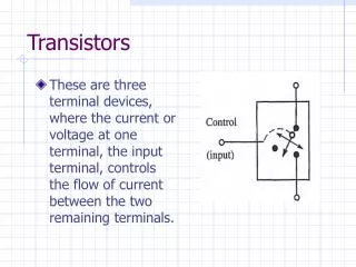
Transistors are scalable electronic switches, made from doped silicon. Silicon forms a crystal, and have no free electrons at low temperature (around 0K). At higher temperatures (300K), thermal energy is sufficient to release some electrons from their covalent bonds. The availability of conducting electrons is, however, limited (more quantitative) because the band-gap energy is high relative to a good conductor (copper).
N P N- and P-type doped silicon are the components necessary to build switching devices, like diodes and transistors. Dopant atoms can integrate with silicon’s crystal lattice, and create additional holes or conducting electrons. Because phosphorus has five valance electrons, an additional weakly bound electron is present when it integrates. Thermal energy frees this electron, producing a large number of conducing electrons in this material, known as N-type. Tri-valent Boron creates a hole upon integration, producing P-type material.
Sets up a field Diffusion Establishes current equilibrium N P N P N P Diffusion Diffusion Si Si Si Si Si Si Field P Si P+ Si P+ Si Si B Si B- Si B- Si Si Si Si Si Si + - The diode device architecture fuses an N and a P-junction together. The NP junction with no voltage applied establishes an equilibrium such that the force of diffusion, which draws electrons into the P-type material, is opposed by the force of the electric field, which draws electrons back into the N-type material. This “equilibrium” electric field represents a potential difference around 0.76V (proven, p. 18 of Electronic Circuit Design and Analysis).
N-type P-type Relative concentration of majority carrier in N-type material: electrons Si Si P Si Si B Diffusion “force” Si Si Relative concentration of minority carrier in P-type material: electrons The N-region contains a higher concentration electrons than the P-region. Electrons diffuse from the N to P-type material.
Electric field (oriented from positive to negative), ~0.75V Electric force (on electrons) due to equilibrium field N-type P-type Electrons Si Si P+ Si Si B- Diffusion “force” Si Si Electrons Diffusion establishes a charge separation, which sets up an electric field. The field exerts a force on the electrons opposite the direction of diffusion.
Electric field (oriented from positive to negative) , ~0.75V Electric force (on electrons) N-type P-type Diffusion “force” Electrons : equilibrium Diffusion continues and the charge separation continues to grow in magnitude, until the force of the electric field due to the charge separation equally opposes the force of diffusion. At this point, there is no net current flow across the junction, and the electron concentration at either side of the junction reaches an equilibrium value.
Reverse Bias Applied Field N P Net Field > Equilibrium Si Si Force P+ Si Si B- Si Si Equilibrium Field, ~0.75V + - In reverse bias voltage, the fields are oriented in the same direction, and the magnitude of the electric field in the space charge region increases above the equilibrium value. This holds back electrons, and no current flows. With forward bias, the net result is that the eclectic field at the junction is lower than the equilibrium value, and electrons diffuse.
Applied electric field from reverse-bias voltage polarity Electric field (oriented from positive to negative) Net electric force due to fields N-type P-type Diffusion “force” Electrons drawn from P-type material near junction Electrons Reverse-bias voltage increases net field at the junction, opposing diffusion. Charges are drawn away from the junction by the field.
Forward Bias Applied Field N P Net Field < Equilibrium Si Si Net diffusion P+ Si Si B- Si Si Equilibrium Field - + In reverse bias voltage, the fields are oriented in the same direction, and the magnitude of the electric field in the space charge region increases above the equilibrium value. This holds back electrons, and no current flows. With forward bias, the net result is that the eclectic field at the junction is lower than the equilibrium value, and electrons diffuse.
Applied electric field from forward-bias voltage polarity Electric field (oriented from positive to negative) Net electric force due to fields N-type P-type Diffusion “force” exceeds the net electric force, electrons diffuse across junction, where electron concentration is above equilibrium Electrons diffuse from junction into the bulk Electrons Forward-biased voltage reduces net field at the junction, reducing the width of the depletion region. The force of diffusion dominates.
Device schematic Transfer function I Two-state: Non-linear response at “on” threshold Vin Output: current Current No current Input: voltage V forward bias V reverse bias Voltage input Sensitive: Only 0.7V “on” threshold I = Is*[ e^(Vin/Vt) -1 ] Is = Reverse bias current, 5*10^(-14)A Vt = Thermal voltage = 0.026 The output is highly responsive to increases in the forward-biased input, above the “cut in” voltage threshold ~0.7V. At zero or reverse bias input voltage, the output current is the very small saturation value, around 5*10^(-14)A. Because the forward bias voltage is included in the exponent, the exponential terms increases with respect to the input voltage. At the cut in voltage ~0.7V, the input voltage driven exponential term begins to dominate the very small reverse bias saturation current term, resulting in the exponential behavior. Physically, this means that diffusion is unrestricted once the forward bias voltage establishes a field that fully counters the built-in equilibrium field.
V=IR I=Vs/R Energy balance: I= -(1/R)*Vd+Vs/R R Diode Vd Voltage Source Vd = Vs Vd KVL (energy balance): Vs=IR+Vd I= -(1/R)*Vd+Vs/R The diode current and voltage are given by the intersection between the circuit load line and the diode performance curve. This intersection, or Q-point, gives the DC voltage and current for the forward-biased diode in the circuit: this intersection identifies the feasible diode operating conditions that also satisfy the energy balance of the circuit.
Voltage drop 0.7V Switch voltage Polarity forward to reverse bias 5V I 4.3V, I=4.3/R 0V, I=0 R R + - Supply : 5V Time + - Zero output A diode circuit can make a switch. If the output is defined as the voltage drop across the resistance, then output is zero in the reverse bias condition (red). This is because the diode is reverse biased in this condition, resulting in no circuit current and no resistor voltage drop.
Supply : 5V R I Vi (1) V (o) Vi (2) A diode circuit can make an AND gate. If both inputs are high (5V), then there is no potential difference across either diode (no voltage difference between input and supply). Neither diode is forward biased, no current flows. Since there is no current in the circuit, there is no voltage drop across the resistance and output voltage is 5V (high). If either input is low, then the diode is forward biased and the voltage drop across the diode will be ~0.7V. Thus, ~4.3V will drop across the resistance, resulting in a 0.7V (low) output.
Vi (1) V (o) Vi (2) R I A diode circuit can make an OR gate. If either input is high (5V), the corresponding diode is forward biased with a 0.7V drop. The output voltage is 4.3V, and the resistance determines the output current (4.3V/R).
N P Net diffusion P+ Si Equilibrium Field Input Voltage - + Resistance, R 10V Supply Voltage, V Voltage Out = Always High A diode in the circuit will not switch the output because the applied field from the supply voltage will over-ride the applied field from the input voltage. The diode is forward biased with respect the supply voltage , so current will always flow through the circuit.
Current through first diode controlled by input voltage Second diode is reverse biased with respect to supply, so no current Input Voltage - + Supply Voltage, V - + Resistance, R 10V Voltage Out = Always Low Adding a second diode establishes a three-terminal device in which the voltage across the first diode is set by the input and unaffected by the supply. The second diode is reverse biased with respect to the supply voltage, which shields the first diode. However, no current will flow through the outer circuit because the second diode is reverse biased.
P N N An NPN junction produces the effect of two opposing diodes in the circuit.
Forward Bias Reverse Bias Applied field from supply voltage Applied field from input voltage P N N Net diffusion Force - Equilibrium Field Equilibrium Field - + Supply Voltage, V Base current Input Voltage - + Resistance, R 10V Voltage Out = Always Low No current flows in the outer circuit because all electrons entering the P-type region exit through P-region lead, and because no current can flow across the reverse biased PN junction Electrons diffuse from N to P-type material, recombine with holes, and exit through the conductor in the P-type material.
P N N Make base thin Net diffusion Force The electron concentration across the P region varies from high at the forward biased junction through which electrons are passing to low at the reverse biased junction, at which no current is flowing. Transistors are designed to allow diffusion of electrons across this concentration gradient, from the emitter across the base and into the collector, thus completing the outer circuit. This is done by making the base thin. The thin base leads to a sharper concentration gradient, and reduces the likelihood of recombination.
N Collector N Emitter P Base Net diffusion Force - Equilibrium Field - + Supply Voltage, V Ib Input Voltage - + Resistance, R 10V Voltage Out = Contollable In a bi-polar junction NPN transistor, electrons are injected into and diffuse through the base to the collector, completing the outer circuit. Many of the electrons will not recombine with holes in the base (P-region) for two reasons. First, the emitter is heavily doped and the base is lightly doped. Second, the P-region is thin. Because there is a concentration gradient across the region, electrons diffuse towards the reverse-biased base-collector junction. The electrons will be captured by the strong electric field at this junction, and will flow into the collector.
Device Transfer Function Energy balance: Ib= -(1/Rb)*Vbe+Vbase/Rb Intersection gives Ib and Vbe Rb B Load line + E Vbe I (base) - Vbase Ib The transistor can be de-coupled into two parts, first one being the base-emitter, which functions like a diode. Diode performance can be determined (along with the base current) by the load line intersection with the diode performance curve.
Energy balance: Vsource = Vt +IcRc C Rc Vout Rb Vt B + + E Vbe I (base) - Vsource Vbase - Ib The current exiting the collector, Ic, is determined by the voltage across base-emitter junction (the input) only. This is because electron injection to the base from the emitter is the limiting factor on the current through the circuit, and base voltage control the degree of electron injection. As a result, Ic is independent of the reverse-bias voltage polarity across the BC junction: if, for example, Rc decreases, the voltage drop across the transistor, Vt, will increase (energy balance). The voltage drop across the BE junction is fixed at 0.7V, for a forward biased diode. Thus, the reverse bias voltage across the BC junction will have to increase. However, this has no affect on the output current. The collector current is related to the base current by a factor B, or gain, which is between 50 – 200 for transistors. The above design is a common emitter (emitter is the common connection) bi-polar junction transistor.
Output Out (Ic) Various inputs (Vbe) C B On E In (Vbe) Vt Vt Off Energy Balance: –(1/Rc)Vt+Vsource/Rc=Ic Vt must be > Vbe, else there is no reverse bias across the base-collector Two elements are necessary for the shared emitter, bi-polar junction NPN transistor. First, there must be reverse bias voltage polarity across the base-emitter junction to capture diffusing electrons in the base. This is represented on the x-axis. The output is weakly dependent upon the degree of reverse bias, reflected by weak slope of each line. But the output will drop off rapidly as if the voltage across the transistor is too low to maintain reverse bias across BE junction. Second, there must be forward-biased input voltage. As the input voltage increases (represented by each curve), the output current increases. The lower line represents zero input voltage, and output is zero, as expected.