Download
1 / 2
20 likes | 35 Views
To show circuit functionality and be readable PCB assembly layout designers in the past worked from schematics that usually drawn in a meaningful way.

E N D
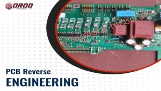
Reverse Engineering of PCB Assembly Turn into Reverse Analysis To show circuit functionality and be readable PCB assembly layout designers in the past worked from schematics that usually drawn in a meaningful way. For instance, angled wires pointing to each other indicates by the cross-page connection. The PCB designers logically made the physical parts placement follow the schematics, and the components that formed functional groupings tended to remain co-located. Usually, the schematics can be read and understood by others, which includes those schematics that were used later to perform troubleshooting, deduce circuit operation, and repair. However, it was relatively easy to recreate a schema from such a PCB assembly. More then, CAE and CAD came along. Into an electronic Etch A Sketch capture tool the art of schematic drawing became debased, whose primary purpose was to create a netlist. So, to complete the planting of the copper traces the PCB designer could use a "rat's nest" on-screen display. In the digitized dumbing-down, any semblance of analog rules or communication between the design engineer and the PCB layout designer was lost. Based on actual PCB placement and package pin-outs, reverse analysis is a two-pass effort requiring an initial physical schematic. Re-drawing the captured circuits in a logical and comprehensible fashion the series of the functional schematic followed. Moreover, the PCB assemblies’ representation is the real schematic. As on the PCB assembly, components drawn in the same orientation and with GDS or EBC physical pins transistors shown in their representative packages. Arranged in the same way relay switches are sown with their terminals as they appear from the top. With the display of functional names and internal logic elements, ICs drawn in their packages. Relating components to a later functional schematic strongly varies on the physical schema, as most of the times a PCB assembly does not have reference designators in the silkscreen. It is impossible to figure out what is going on electrically. However, the result is a very readable and understandable depiction once this has been re-drawn into a meaningful functional
schematic. Temporarily color-coding the nets on the physical drawing make the transfer to the technical drawing less prone to error and when dragged around for readability, flexible wires follow the components. Unfortunately, when an element is rotated or flipped, TinyCAD does not keep wires connected. For instance, you have your physical schematic drawn out on a single page, with everything scrunched up close together, impossible to make any sense of the actual electrical functions and long runs of closely spaced wires. Setting its color to bright purple, width to 25 and apply to the entire net with just a click on a fence, suddenly that net jumps off the page at you. Additionally, any net throughout the page with the same name attached will also brighten into visibility. Hence, an individual should have some form of revision control to keep track of the latest updated drawing when others need access to it. So is your PCB assembly no longer manufactured or you need any replacements or capacity additions? Lost your drawings or schematics from corrupted files? Reverse engineer is the best solution. Reverse engineering of PCB’s is one ofPCC specialties and our PCB and PCA knowledge with long years of manufacturing experience, has enabled us to provide optimum PCB Reverse Engineering Services. With proficiency and understanding of PCB Reverse Engineering Process, PCC has a dedicated team of engineers following IPC design specifications and work on simple to the most complex PCB/PCA projects