Download
1 / 6
60 likes | 64 Views
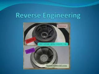
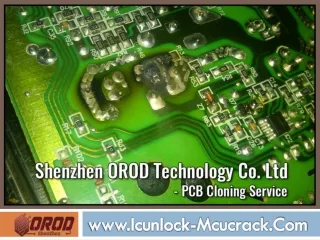
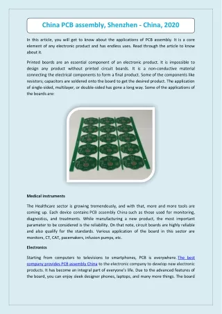
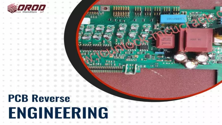
PCB reverse engineering (PCB Copy) is a significant part of PCB design. One of the finest benefits of using printed circuit boards is the amount of time that can be saved. Connecting components conventionally takes a lot of time, whereas the circuit board will take far less time to assemble once the design is total. http://icunlock-mcucrack.com/case/omap4430-based-third-order-hdi-pcb-reverse-engineering/

E N D
Today's demands in PCB reverse engineering • PCB reverse engineering is to first withdraw the components on the PCB circuit board to make a BOM list. • PCB reverse engineering empty board into a picture, and reinstate it to a pcb board drawing file through the copying software. • Computing the PCB board drawing file to the PCB board factory to make the board (PCBA).
Any electronic product copy and electronic product cloning can be completed through PCB copy board technology. • The motive of PCB copy is sometimes to modify the PCB, which is to conduct alter technology research on the designed PCB board. • After mention to a lot of information, the process of PCB reverse engineering is outline as follows:
The first step is to get a PCB reverseengineering first record the model, framework, and positions of all crucial parts on paper. • The second steg is to detach all the components and take out the tin in the PAD hole. • The third stage is to modify the contrast and brightness of the canvas to make the part with copper film and the part without copper film have a strong contrast,
Phone Whatsapp: +86-13378667812 E-mail: orod@chip-programmer.com