Download
1 / 161
1.66k likes | 1.89k Views
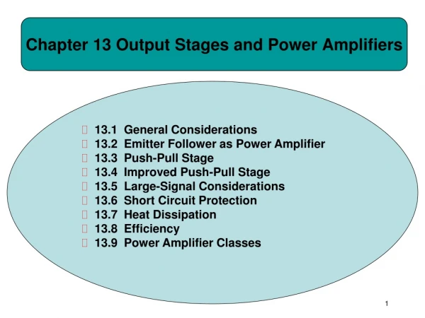
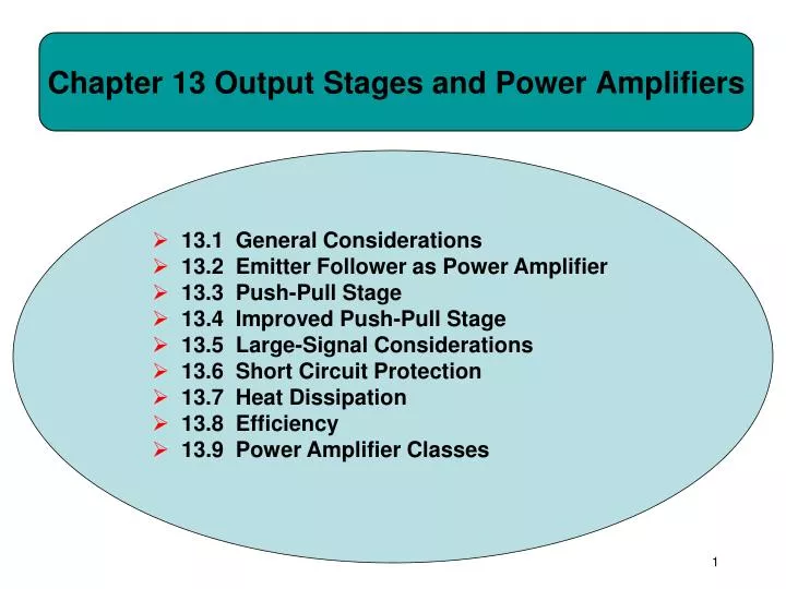
Chapter 13 Output Stages and Power Amplifiers. 13.1 General Considerations 13.2 Emitter Follower as Power Amplifier 13.3 Push-Pull Stage 13.4 Improved Push-Pull Stage 13.5 Large-Signal Considerations 13.6 Short Circuit Protection 13.7 Heat Dissipation

E N D
Chapter 13 Output Stages and Power Amplifiers • 13.1 General Considerations • 13.2 Emitter Follower as Power Amplifier • 13.3 Push-Pull Stage • 13.4 Improved Push-Pull Stage • 13.5 Large-Signal Considerations • 13.6 Short Circuit Protection • 13.7 Heat Dissipation • 13.8 Efficiency • 13.9 Power Amplifier Classes
Why Power Amplifiers? • Drive a load with high power. • Cell phone needs 1W of power at the antenna. • Audio system needs tens to hundreds Watts of power. • Ordinary Voltage/Current amplifiers are not equipped for such applications CH 13 Output Stages and Power Amplifiers
Chapter Outline CH 13 Output Stages and Power Amplifiers
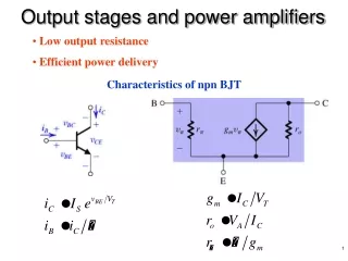
Power Amplifier Characteristics • Experiences small load resistance. • Delivers large current levels. • Requires large voltage swings. • Draws a large amount of power from supply. • Dissipates a large amount of power, therefore gets “hot”. CH 13 Output Stages and Power Amplifiers
Power Amplifier Performance Metrics • Linearity • Power Efficiency • Voltage Rating CH 13 Output Stages and Power Amplifiers
Emitter Follower Large-Signal Behavior I • As Vin increases Vout also follows and Q1 provides more current. CH 13 Output Stages and Power Amplifiers
Emitter Follower Large-Signal Behavior II • However as Vin decreases, Vout also decreases, shutting off Q1 and resulting in a constant Vout. CH 13 Output Stages and Power Amplifiers
Example: Emitter Follower CH 13 Output Stages and Power Amplifiers
Linearity of an Emitter Follower • As Vin decreases the output waveform will be clipped, introducing nonlinearity in I/O characteristics. CH 13 Output Stages and Power Amplifiers
Push-Pull Stage • As Vin increases, Q1 is on and pushes a current into RL. • As Vin decreases, Q2 is on and pulls a current out of RL. CH 13 Output Stages and Power Amplifiers
I/O Characteristics for Large Vin Vout=Vin-VBE1 for large +Vin Vout=Vin+|VBE2| for large -Vin • For positive Vin, Q1 shifts the output down and for negative Vin, Q2 shifts the output up. CH 13 Output Stages and Power Amplifiers
Overall I/O Characteristics of Push-Pull Stage • However, for small Vin, there is a dead zone (both Q1 and Q2 are off) in the I/O characteristic, resulting in gross nonlinearity. CH 13 Output Stages and Power Amplifiers
Small-Signal Gain of Push-Pull Stage • The push-pull stage exhibits a gain that tends to unity when either Q1 or Q2 is on. • When Vin is very small, the gain drops to zero. CH 13 Output Stages and Power Amplifiers
Sinusoidal Response of Push-Pull Stage • For large Vin, the output follows the input with a fixed DC offset, however as Vin becomes small the output drops to zero and causes “Crossover Distortion.” CH 13 Output Stages and Power Amplifiers
Improved Push-Pull Stage VB=VBE1+|VBE2| • With a battery of VB inserted between the bases of Q1 and Q2, the dead zone is eliminated. CH 13 Output Stages and Power Amplifiers
Implementation of VB • Since VB=VBE1+|VBE2|, a natural choice would be two diodes in series. • I1 in figure (b) is used to bias the diodes and Q1. CH 13 Output Stages and Power Amplifiers
Example: Current Flow I If Vout=0 & β1=β2>>1 => IB1=IB2 Iin CH 13 Output Stages and Power Amplifiers
Example: Current Flow II VD1≈VBE → Vout≈Vin If I1=I2 & IB1≈IB2 → Iin=0 when Vout=0 CH 13 Output Stages and Power Amplifiers
Addition of CE Stage • A CE stage (Q4) is added to provide voltage gain from the input to the bases of Q1 and Q2. CH 13 Output Stages and Power Amplifiers
Bias Point Analysis VA=0 Vout=0 IC1=[IS,Q1/IS,D1]×[IC3] • For bias point analysis, the circuit can be simplified to the one on the right, which resembles a current mirror. • The relationship of IC1 and IQ3 is shown above. CH 13 Output Stages and Power Amplifiers
Small-Signal Analysis AV=-gm4(rπ1||rπ2)(gm1+gm2)RL • Assuming 2rD is small and (gm1+gm2)RL is much greater than 1, the circuit has a voltage gain shown above. CH 13 Output Stages and Power Amplifiers
Output Resistance Analysis • If β is low, the second term of the output resistance will rise, which will be problematic when driving a small resistance. CH 13 Output Stages and Power Amplifiers
Example: Biasing CE AV=5 Output Stage AV=0.8 RL=8Ω βnpn=2βpnp=100 IC1≈IC2 CH 13 Output Stages and Power Amplifiers
Problem of Base Current • 195 µA of base current in Q1 can only support 19.5 mA of collector current, insufficient for high current operation (hundreds of mA). CH 13 Output Stages and Power Amplifiers
Modification of the PNP Emitter Follower • Instead of having a single PNP as the emitter-follower, it is now combined with an NPN (Q2), providing a lower output resistance. CH 13 Output Stages and Power Amplifiers
Example: Input Resistance CH 13 Output Stages and Power Amplifiers
Additional Bias Current • I1 is added to the base of Q2 to provide an additional bias current to Q3 so the capacitance at the base of Q2 can be charged/discharged quickly. CH 13 Output Stages and Power Amplifiers
Example: Minimum Vin Min Vin≈0 Vout≈|VEB2| Min Vin≈VBE2 Vout≈|VEB3|+VBE2 CH 13 Output Stages and Power Amplifiers
HiFi Design • Using negative feedback, linearity is improved, providing higher fidelity. CH 13 Output Stages and Power Amplifiers
Short-Circuit Protection • Qs and r are used to “steal” some base current away from Q1 when the output is accidentally shorted to ground, preventing short-circuit damage. CH 13 Output Stages and Power Amplifiers
Emitter Follower Power Rating • Maximum power dissipated across Q1 occurs in the absence of a signal. CH 13 Output Stages and Power Amplifiers
Example: Power Dissipation Avg Power Dissipated in I1 CH 13 Output Stages and Power Amplifiers
Push-Pull Stage Power Rating • Maximum power occurs between Vp=0 and 4Vcc/π. CH 13 Output Stages and Power Amplifiers
Example: Push-Pull Pav If Vp = 4VCC/π→ Pav=0 Impossible since Vp cannot go above supply (VCC) CH 13 Output Stages and Power Amplifiers
Heat Sink • Heat sink, provides large surface area to dissipate heat from the chip. CH 13 Output Stages and Power Amplifiers
Thermal Runaway Mitigation • Using diode biasing prevents thermal runaway since the currents in Q1 and Q2 will track those of D1 and D2 as long as theieIs’s track with temperature. CH 13 Output Stages and Power Amplifiers
Efficiency Emitter Follower Push-Pull Stage I1=VP/RL I1=VP/RL • Efficiency is defined as the average power delivered to the load divided by the power drawn from the supply CH 13 Output Stages and Power Amplifiers
Example: Efficiency Emitter Follower VP=VCC/2 Push-Pull I1=(VP/RL)/β CH 13 Output Stages and Power Amplifiers
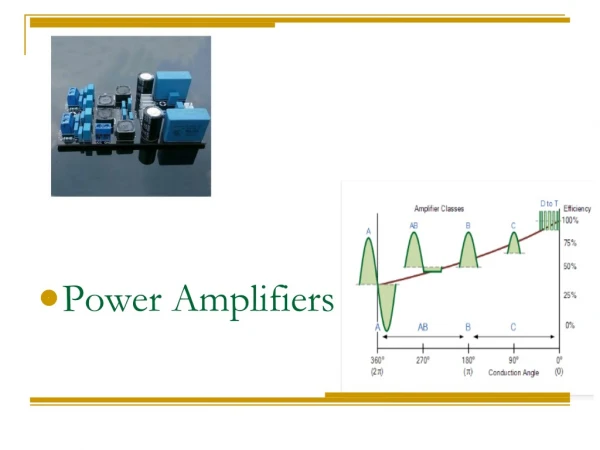
Power Amplifier Classes Class A: High linearity, low efficiency Class B: High efficiency, low linearity Class AB: Compromise between Class A and B CH 13 Output Stages and Power Amplifiers
Chapter 14 Analog Filters • 14.1 General Considerations • 14.2 First-Order Filters • 14.3 Second-Order Filters • 14.4 Active Filters • 14.5 Approximation of Filter Response
Outline of the Chapter CH 14 Analog Filters
Why We Need Filters • In order to eliminate the unwanted interference that accompanies a signal, a filter is needed. CH 14 Analog Filters
Filter Characteristics • Ideally, a filter needs to have a flat pass band and a sharp roll-off in its transition band. • Realistically, it has a rippling pass/stop band and a transition band. CH 14 Analog Filters
Example: Filter I Given: Adjacent channel Interference is 25 dB above the signal Design goal: Signal to Interference ratio of 15 dB Solution: A filter with stop band of 40 dB CH 14 Analog Filters
Example: Filter II Given: Adjacent channel Interference is 40 dB above the signal Design goal: Signal to Interference ratio of 20 dB Solution: A filter with stop band of 60 dB at 60 Hz CH 14 Analog Filters
Example: Filter III • A bandpass filter around 1.5 GHz is needed to reject the adjacent Cellular and PCS signals. CH 14 Analog Filters
Classification of Filters I CH 14 Analog Filters
Classification of Filters II Discrete-time Continuous-time CH 14 Analog Filters
Classification of Filters III Passive Active CH 14 Analog Filters
Summary of Filter Classifications CH 14 Analog Filters