1 / 13
130 likes | 136 Views
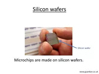
Silicon wafers exist in a wide range of sizes, and various varieties of diameters. The variety of sizes allows the tech industry to have the freedom to use a specifically sized wafer in various gadgets.

E N D
9 Facts about Silicon Wafers Silicon Specialist LLC
Silicon has helped revolutionize the tech industry. Due to its properties, silicon has become increasingly popular to be used in modern gadgets. The existence of handy and compact devices such as smartphones, computers, and televisions is because of silicon because their building blocks i-e integrated circuits (ICs) are made of silicon. Being the second most abundant element in the world and flexible, silicon makes an ideal element to make tech gadgets. It is flexible in terms of availability and versatile, which makes it perfect for use in technology items and other everyday materials. In this article, we have discussed nine really interesting facts about silicon wafers which form the basis of sophisticated gadgets in the modern world.
Basis for Semiconductors Silicon Wafers are also known as semiconductors. They possess the properties of both a conductor and an insulator, as they are a hybrid of insulators and metals that would either be conducted by electricity or not. However, the manufacturing of semiconductors does not merely base on silicon. Instead, other elements such as Germanium, Indium Phosphide, Sapphire, and Quartz also go into the making of these.
Wide range of Varieties Silicon wafers exist in a wide range of sizes, and various varieties of diameters. The variety of sizes allows the tech industry to have the freedom to use a specifically sized wafer in various gadgets. You can pick the wafer based on your requirements as per the diameter availability. The very first semiconductor wafer had only a 1-inch diameter. This was back in the 1960s. However, today you can have wafers up to the diameter of 18 inches. While sometimes, the size of a gadget requires a specifically sized wafer, at other times, the wafer diameter size determines the size of item it has been used in.
Leading Market in the World With 51% of the global shares of silicon wafers, the United States dominates the market of silicon wafers. The main reason behind the USA’s lead in the field of silicon wafers is its progressive and industrialized economy that is far too ahead to be competed with by other countries. However, various other factors also contribute to keeping them at the top of their game. The silicon wafers are also supplied to other countries like Japan, Germany, and Russia for their use.
Desirable Purity Level For a simplified technology that uses a repeated application, those silicon wafers are preferred which have higher “nines” purity (%99.99999). The nines purity percentage in wafers makes it more desirable for use in integrated circuits.
Purification Method Silicon wafers are made in a very interesting way. First, the obtained silicon is melted and allowed to re-solidify for 100% purity. In the past, aggressive methods aimed at crushing metallurgical grade silicon which was then dissolved in acid to be purified. Mixing of silicon with acid causes the impurity-defined silicon to get more purified.
Discovery of Silicon Silicon, the main constituent of semiconductor wafers, was discovered by Swedish chemist Jacob Berzelius, in 1824. To obtain silicon, potassium chips present in silica flasks are heated, and then residual by-products are separated to obtain pure silicon. In modern times, sand with carbon is heated to a high temperature, up to 2200 degrees Celsius, to obtain pure silicon.
Water’s role in the production During production, water plays a significant role. Being a major solvent for a variety of substances, water is used during silicon manufacturing for the same reason. Up to 4.8 million gallons are required every day by the production facilities to manufacture silicon in sufficient quantity. Therefore, industries spend around $1 billion on the water to form silicon wafers manufacturing.
Temperature Resistance Silicon is a highly durable substance which makes it ideal to be used in semiconductor wafers in technologies all around the world. With a high-temperature resistance, it is considered ideal to be used in tools that are subject to high temperatures. They are suitable for highly demanding interiors of processing units and mobile devices.
Preferred for ICs In the past vacuum tubes were used for integrated circuits, however, they have been replaced with silicon wafers now. With their highly desirable properties, silicon wafers have paved the way for the tech revolution. They are more reliable and compact compared to the bulky vacuum tubes of the ’50s.
Silicon Specialists LLC For high quality, SILICON WAFERS CA (Si wafers), visit our website. Whether you want standardized wafers or customized ones, we are equally expert in manufacturing and distributing them.
THANK YOU • Address: 2487 Industrial Pkwy W, Hayward, CA 94545 • Email: mcgnsmith@yahoo.com • Number: (510) 732-9796 • Website: www.siliconspecialists.com