Download
1 / 23
230 likes | 328 Views
LHCb Vertex Detector and Beetle Chip. Outline: Introduction VE rtex LO cator Pile-up trigger Radiation hardness of electronics Architecture of Beetle chip Test beam results Conclusions & outlook. The LHCb Vertex Locator (VELO).

E N D
LHCb Vertex Detector and Beetle Chip • Outline: • Introduction VErtex LOcator • Pile-up trigger • Radiation hardness of electronics • Architecture of Beetle chip • Test beam results • Conclusions & outlook 1
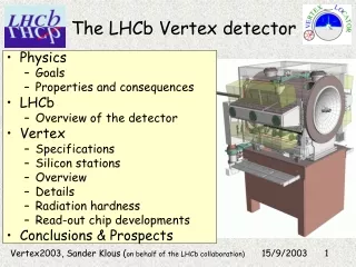
The LHCb Vertex Locator (VELO) The VELO provides an accurate reconstruction of primary & secondary (displaced) vertices 2
Vertex Locator • 21 VELO + 2 Pile-Up stations • R/ Silicon strip detectors • ~ 180k strips • Typical hit resolution 8 mm • CO2 cooling: 2 kW @-10 C • Radiation dose 100 kGy (4 years) • Vacuum feedthrough: 20k pins 3
RF shielding • Secondary vacuum • 26 A peak current through box • 300 mm Al foil • 11 mm hole for the beam !! • Detectors are retracted during beam injection 4
Pile-up trigger (veto) ZPV - ZA RA = ZPV - ZB Rb = k • Detection of multiple primary vertices • R-strip detectors only • L0-trigger: prompt binary signals needed • Processing time < 2.2 s • Logic OR of 4 detector signals in Beetle • 1024 binary signals @ 80 Mbit/sec • Special (complex) hybrid • Connectivity challenge ! 5
Front-end chip requirements Pulse from charge sensitive amplifier • 40 MHz sampling rate • Peaking time < 20 ns • Remainder of peak after 25 ns < 30 % • (spill over) • S/N > 14 (300 mm Si) • L0-trigger rate: 1.1 MHz => • Readout time 900 ns • Trigger latency up to 4 ms • Buffering of 16 events • Power consumption < 6 mW / channel • Radiation hardness >100 kGy time 6
Radiation hardness of CMOS V+ + + + + Problem: Single Event Upsets (SEU) i.e. bit-flips Cure: Triple redundancy + majority voting for all registers Problem: Hole trapping in SiO2 (Total Ionizing Dose) Cure: Use deep submicron process + special layout techniques MOS transistor characteristics are determined by width (W) and length (L) Gate oxide 7
Radiation hardness(2) ++ ++ • Hole trapping => threshold shift • Deep Sub Micron process => thinner gate oxide • Tox < 10 nm : tunneling decreases the • amount of trapped holes in the gate-oxide • Solution to parasitic transistors: enclosed layout • (only for nMOS) • Guard rings around nMOS Field oxide • Disadvantages of enclosed layout: • Larger area / capacitance • No “long” transistors possible 8
Beetle functional diagram Beetle chip is designed in 0.25 mm technology Readout (4x) Pipeline (186 deep) Front-end (128 x) comparator 9
Beetle front-end Pre-amplifier: Ipre thermal noise power Shaper: slower pulse: noise spillover • Pulse shape depends on: • Shaper feedback resistance (Vfs) • Shaper current (Isha) Noise is related to the current in the pre-amplifier (Ipre) 20 ns 25 + 40 ns 10 ns 10
Layout of beetle • Beetle: • Designed by ASIC lab • Heidelberg and NIKHEF • 0.25 mm CMOS technology • Pipeline depth 186 cells • Size (5.5 x 6.1) mm2 Front-end (128 x) Pipeline cells 11
Radiation hardness test Vout [V] time [ns] Single chips were tested with X-ray facility at CERN • Beetle showed full functionality up to 300 kGy (12 LHCb years): • All digital functions worked up to 450 kGy • Analog performance degradations are small 12
Hybrid & Silicon 42 mm 8 mm • Micron PR02-R detector • Thickness: 300 mm • 2048 strips • pitch: 40 – 92 mm • length: 6.4 – 66.6 mm • angular coverage 182° • 2 layer pitch adapter • 16 Beetle chips • High yield • 4 layer hybrid (NIKHEF design) • 75 mm kapton / layer • 17 mm copper / layer 13
Test beam setup time Trigger scintillators 120 GeV pions / muons X-Y Si tracking station Hybrid under test • “Continuous” beam => no fixed relation between • particle and Beetle clock signal (40 MHz) • Readout 8 time samples of Beetle • Measure time between trigger and next Beetle clock Collected > 10 Million events in 4 days 14
Pulse shape analysis Noise distribution s = 1 Most probable value Data after baseline correction & common mode noise subtraction 15
Pulse shape analysis (2) Peak height (Signal) Spill over 25ns Rise time (10 to 90 %) 16
S/N results • The new design of the silicon sensor will have only 45 strips • => expected S/N of long strips > 15 Short strips: • Sstrip/Nstrip = 19 • Spill over = 32 % Long strips: • Sstrip/Nstrip = 13 • Spill over = 37 % 17
Conclusions • Radiation hardness of Beetle demonstrated up to 300 kGy • Performance degradation due to hybrid is minimal • Pulse shape characteristics: • Spill over < 30 % • S/N > 15 • Beetle is compliant withall LHCb requirements • Beetle was chosen by VELO group • Inner tracker will also use Beetles 18
Outlook • Next version of Beetle (1.2) + next version of hybrid is planned to be tested in the test beam of summer 2003 • Small design improvements => new Beetle (1.3) submission in spring 2003 • The more complex Pile-Up hybrid is currently under construction (4 times more signals!), to be tested 19
Radiation effects Total Dose effects Single Event effects Ionising Bulk damage Hole trapping (SiO2) Non-Ionising Bulk damage Upsets Yes Triple redundancy +majority voting Damage Latch-up No problem For LHCb Silicon Detectors Readout chips 22