Download
1 / 14
150 likes | 257 Views
Explore the characteristics and operation regions of JFET and MOSFET for amplifier design. Learn about structure, parameters, and transfer curves in this detailed guide.

E N D
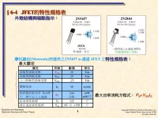
2N2844 外殼22-03, 形態12 TO-18 (TO-226AA) (外殼) 3 汲極 2 閘極 1 源極 一般用途之 p-通道 JFETs (頂帽連接器之型態) 2N5457 外殼29-04, 形態5 TO-92 (TO-226AA) 1 汲極 3 閘極 2 源極 JFETs 一般用途 N-通道-空乏 Boylestad and NashelskyElectronic Devices and Circuit Theory Copyright ©2006 by Pearson Education, Inc.Upper Saddle River, New Jersey 07458All rights reserved. § 6-4 JFET的特性規格表 • 外殼結構與端點指示: • 摩托羅拉(Motorola)所提供之2N5457 n-通道 JFET 之特性規格表: 最大功率消耗方程式:PD=VDSID 1
Boylestad and NashelskyElectronic Devices and Circuit Theory Copyright ©2006 by Pearson Education, Inc.Upper Saddle River, New Jersey 07458All rights reserved. § 6-4 JFET的特性規格表 2
夾止範圍之軌跡 (IDmax) 歐 姆 區 放大器設計 之 正常操作區域 Boylestad and NashelskyElectronic Devices and Circuit Theory Copyright ©2006 by Pearson Education, Inc.Upper Saddle River, New Jersey 07458All rights reserved. § 6-4 JFET的特性規格表 • 線性放大器設計 之 正常操 作範圍: • •特性規格表 與 每一VGS 大小 之夾止範 • 圍所定義的曲線 可規範 汲極特性之線 • 性放大操作區域。 • •歐姆區 定義 每一VGS 之 最小允許VDS • 之值。 3
VGS= 0V→ID= IDSS ID = ½ IDSS → VGS≅ 0.3Vp →VGS= 0V,-0.5V,-1V,-1.5V,-2V 此為 n-通道裝置, 設定顯示 五步級 --- 十步級? (每步級) ID = 0mA→ VGS= Vp Boylestad and NashelskyElectronic Devices and Circuit Theory Copyright ©2006 by Pearson Education, Inc.Upper Saddle River, New Jersey 07458All rights reserved. § 6-5 儀表 • 2N4416 JFET 顯示在 曲線循跡器之汲極特性: • ps:當VGS 愈變愈負時,曲線間的距離愈縮減。 4
待定參數 分析結構起點→ Boylestad and NashelskyElectronic Devices and Circuit Theory Copyright ©2006 by Pearson Education, Inc.Upper Saddle River, New Jersey 07458All rights reserved. § 6-6 重要關係式 5
(汲極) (絕緣用薄層) n 通道 金屬接點 (Sub Strate) 基體 SS (閘極) P 基體 有時內↓ s 矽 基 板 n 型區域 (源極) Boylestad and NashelskyElectronic Devices and Circuit Theory Copyright ©2006 by Pearson Education, Inc.Upper Saddle River, New Jersey 07458All rights reserved. § 6-7 空乏型 MOSFET • MOSFETs分為 空乏型 與 增強型;這兩種MOSFET有 不同特性 與 不同基本操 作模式。 • 空乏型MOSFET 與 JFET 介於 截止與飽和 IDSS 之間 有相同特性,但有 增加延 伸至相反VGS 極性區域 之特性。 • 基本結構 (n-通道 空乏型 MOSFET): • •SiO2是一種 特殊的絕緣體 被稱為 • 電介質,當 有外加電場時 即在 電 • 介質內 建立起 反向電場。 • •SiO2之絕緣層 導致 裝置極高之輸 • 入阻抗,值與典型之JFET差不多。 • → 直流偏壓結構下 IG = 0A • •閘極與通道間 的絕緣層 導致裝置 • 之別名: 絕緣閘FET或 IGFET 6
基本操作與特性: • (n-通道 空乏型 MOSFET) • •VGS偏壓愈負,電子與電洞復合率愈高 ⇒ID↓。(如右圖) • ∴ ,VGS= 0V→ ID= IDSS,VGS< 0V→ ID < IDSS SiO2 層 n-通道 復合過程 (VGS<0) p-材料基體 電洞被吸 引至閘極 之負電位 金屬接點 電子被閘極之 負電位所排斥 Boylestad and NashelskyElectronic Devices and Circuit Theory Copyright ©2006 by Pearson Education, Inc.Upper Saddle River, New Jersey 07458All rights reserved. § 6-7 空乏型 MOSFET 7
空乏區 增強區 ↑ 增強區 ↓ 空乏區 Boylestad and NashelskyElectronic Devices and Circuit Theory Copyright ©2006 by Pearson Education, Inc.Upper Saddle River, New Jersey 07458All rights reserved. § 6-7 空乏型 MOSFET • •其 汲極電流 與 轉移曲線 和 JFET 相似。 • •VGS>0,將從 p-型基體吸引更多的自由載子-電子(由於逆向漏電流之故), • 同時加速質點間碰撞產生新載子。 ⇒ VGS>0↑,ID ⇈ > IDSS (如圖) • •因 ID ⇈> IDSS,故須知道最大汲極電流額定值。 • •基於 通道中自由載子數 是否 “增強” ? • → 在 汲極 或 轉移特性曲線 上,正閘極電壓區域 被稱為 增強區 • ,截止與IDSS 飽和值間區域 被稱為 空乏區 8
⑤ 解:蕭克萊方程式 ①VGS = 0V→ ID = IDSS = 10mA ②ID = 0mA→ VGS= Vp = -4V ③VGS = ½ Vp = ½ (-4V)= -2V → ID = ¼ IDSS = ¼ (10mA)= 2.5mA ④ID = ½ IDSS = ½ (10mA)= 5mA → VGS≅ 0.3Vp = 0.3(-4V)= -1.2V ⑤因VGS>0↑, ID ⇈>IDSS ,故值不可代太大 VGS = +1V→ 將①~⑤點繪製曲線→右圖轉移曲線 ① ④ ③ ② Boylestad and NashelskyElectronic Devices and Circuit Theory Copyright ©2006 by Pearson Education, Inc.Upper Saddle River, New Jersey 07458All rights reserved. § 6-7 空乏型 MOSFET 例題 6.3:畫出 IDSS =10mA 及 VP = -4V,n-通 道空乏型 MOSFET之轉移特性。 9
IDSS= 6mA ⓐ ⓑ ⓒ § 6-7 空乏型 MOSFET • p-通道 空乏型 MOSFET: • •結構 與 n-通道 相反,即有 n-型基體 與 p-型通道。----ⓐ • •所有 電壓極性 與 電流方向 均相反。(VDS<0→ID >0且VGS有相反極性)---ⓐ,ⓒ • •VGS之變號 將導致 轉移特性 (對於ID 軸) 鏡像反射。(VGS↓⇒ ID↑)----ⓑ • •蕭克萊方程式 仍可適用。 10
n-通道 p-通道 § 6-7 空乏型 MOSFET • 符號: • •符號 反映 裝置之真實結構。 • •閘極與通道間所缺乏的直接連接 (由於閘極絕緣) 用 符號之閘極與其他端子 • 間的間隔 來表示。 • •每種型態的通道 有 兩種符號,此反映某些情況下 基體可外接。 11
2N3797 外殼22-03, 形態2 TO-18 (TO-206AA) 3 汲極 2 閘極 1 源極 MOSFETs 低功率音顏 N-通道-空乏型 Boylestad and NashelskyElectronic Devices and Circuit Theory Copyright ©2006 by Pearson Education, Inc.Upper Saddle River, New Jersey 07458All rights reserved. § 6-7 空乏型 MOSFET • 規格表 與 外殼結構: 12
Boylestad and NashelskyElectronic Devices and Circuit Theory Copyright ©2006 by Pearson Education, Inc.Upper Saddle River, New Jersey 07458All rights reserved. § 6-7 空乏型 MOSFET •因 ID 可超過 IDSS,故規格表通常會提供 某VGS >0時 之典型 ID 值。 13
Boylestad and NashelskyElectronic Devices and Circuit Theory Copyright ©2006 by Pearson Education, Inc.Upper Saddle River, New Jersey 07458All rights reserved. § 6-7 空乏型 MOSFET 14