100nm
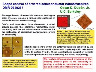
>10 5 islands. b. a. 0.25 mm. d. c. 10x10 μ m 2. 100nm. Shape control of ordered semiconductor nanostructures DMR- 0349257 Oscar D. Dubón, Jr. U.C. Berkeley.

100nm
E N D
Presentation Transcript
>105 islands b a 0.25 mm d c 10x10 μm2 100nm Shape control of ordered semiconductor nanostructures DMR-0349257 Oscar D. Dubón, Jr. U.C. Berkeley The organization of nanoscale elements into higher order systems remains a fundamental challenge in nanoscience and nanotechnology. Dubón and co-workers have discovered a novel growth process that combines rudimentary metal patterning and natural self-assembly processes for the realization of germanium nanostructure arrays on silicon (Fig. 1). Figure 1. (left) Optical diffraction from Au-patterned Si covered with over 100,000 Ge islands. (right) Representative atomic force microscopy (AFM) zoom-in image of Ge islands that have ordered into a 2D square lattice (height scale=100 nm). The color (red) in the left image arises from the island spacing. Island-shape control within the patterned region is achieved by the choice of patterned metal species and crystallographic orientation of the Si surface (Fig. 2). These investigations suggest an intimate relationship between Si-Ge intermixing and island morphology. The surface-diffusion-based dynamics of the ordering process point to the possibility of forming a variety of nanostructure arrays in this and other semiconductor systems. Figure 2. Island shapes (AFM phase images) for different metal-species/Si-orientation combinations: (a) Au/Si(001), (b) Au/Si(111), (c) Sn/Si(110), and (d) Au/Si(110) .
Shape control of ordered semiconductor nanostructures DMR-0349257 Oscar D. Dubón, Jr. U.C. Berkeley Education, training, outreach • Integrating research concepts in the classroom—Whether in graduate school or in industry, new college graduates will tackle problems requiring innovative solutions. The successful engineer and future scientist must be able to gather information from a wide variety of sources, synthesize new concepts from this information and convey his/her findings to a technical community and even the public at large. In the capstone course taught by Dubón, engineering seniors perform advanced library research, carry out peer collaborations and reviews, analyze original data produced in Dubón's research labs, and write a technical paper. These activities cultivate important skills that will enable students to better meet challenges in science and technology. • Training the future scientists through cutting-edge research experiences—A major objective of this project is to train future scientists and engineers, who will become leaders on the global stage. Both graduate and undergraduate students conduct original research and present their work at scientific conferences. In addition, students are encouraged to expand their scientific horizons through programs such as NSF's East Asian and Pacific Institutes (EAPSI) Program. • Reaching audiences beyond the classroom and laboratory—Key to developing a strong, diverse workforce is to build an effective pipeline across education levels. To this end, Dubón has participated in the Summer Undergraduate Program in Engineering Research at Berkeley (SUPERB), a program designed to provide research opportunities in engineering to students who have been historically underrepresented. As a panelist, invited speaker, and SUPERB executive committee member, Dubón has sought to share his experiences and insights with program participants. In addition, Dubón served as a session co-organizer and co-chair (with Dr. J. Santiago-Aviles and Dr. L. Martinez-Miranda) for the 2004 National Meeting of the Society for the Advancement of Chicanos and Native Americans in Science. The session "Engineering: Applied Physics, Materials Science, and Biophotonics" was sponsored in part by NSF.