CLOCK GENERATION MODULE (CGM)
CLOCK GENERATION MODULE (CGM). IRQ. LVI. Direct Memory Access Module (DMA). System Integration Module (SIM). Clock Generation Module (CGM). Timer Interface Module (TIM). 68HC08 CPU. RESET. COP. BREAK. Internal Bus (IBUS). Random Access Memory (RAM). Serial

CLOCK GENERATION MODULE (CGM)
E N D
Presentation Transcript
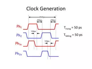
IRQ LVI Direct Memory Access Module (DMA) System Integration Module (SIM) Clock Generation Module (CGM) Timer Interface Module (TIM) 68HC08 CPU RESET COP BREAK Internal Bus (IBUS) Random Access Memory (RAM) Serial Peripheral Interface (SPI) Electronically Programmable ROM Monitor ROM Serial Communications Interface (SCI) Clock Generation Module • Generates base clock frequency for MPU • Two selectable clock sources • Crystal Oscillator • Phase Lock Loop (PLL) • Uses Crystal Oscillator to produce faster clock rate • Output used by System Integration • All sub systems use the system clock for timing • Except Serial Communications Module • Uses Crystal Oscillator frequency
CGM Block Diagram CRYSTAL OSCILLATOR OSC2 CGMXCLK TO SIM, SCI CLOCK OSC1 A CGMOUT SELECT TO SIM CIRCUIT B S* *When S = 1, CGMOUT = B SIMOSCEN CGMRDV CGMRCLK BCS USER MODE V CGMXFC V DDA SS PTC3 VRS[7:4] MONITOR MODE VOLTAGE PHASE LOOP CONTROLLED DETECTOR FILTER OSCILLATOR PLL ANALOG CGMINT LOCK BANDWIDTH INTERRUPT DETECTOR CONTROL CONTROL LOCK AUTO ACQ PLLIE PLLF MUL[7:4] CGMVDV CGMVCLK FREQUENCY DIVIDER
Crystal Oscillator • External crystal is connected between OSC1 and OSC2 • CGMXCLK is oscillator clock output • Equal to external crystal frequency • 4 x internal bus frequency (if selected) • WHEN VCO IS USED TO GENERATE SYSCLK, THE CRYSTAL IS: • Buffered to produce CGMRCLK • Reference frequency for PLL circuit • SIM module can enable/disable oscillator via SIMOSCEN line • Stops crystal oscillator and PLL module
Phase Lock Loop Module • PLL consists of • Bandwidth programmable Voltage Controlled Oscillator (VCO) • Modulo programmable VCO frequency divider • Phase detector • Loop filter • Lock Detector • Operate in Acquisition Mode or Tracking Mode • CGMVCLK is PLL module output • Exact integral multiple of CGMXCLK • 4 x internal bus frequency (if selected)
Programmable VCO • Generates CGMVCLK based on • Frequency divider • Divides frequency producing faster clock • Multiplier select bits control frequency division • Phase detector • Compares CGMXCLK and output of Frequency divider • Detects phase error • Generates correction pulse • Loop filter • Translates phase detector correction pulse into voltage correction for VCO • Programmable bandwidth to improve noisy immunity • VCO range bits determine bandwidth limits
Sequence for PLL Frequency Calculations • Goal: 4MHz bus frequency from a 2 MHz crystal. • 1. Select a desired bus frequency, FBUSDES. FBUSDES = 4 MHz • 2. Calculate desired VCO frequency(four times the desired bus frequency),FVCLKDES FVCLKDES = 4 x FBUSDES FVCLKDES = 4 x FBUSDES = 4 x 4 MHz = 16 MHz • 3. Choose a practical PLL Reference frequency, FRCLK. FRCLK = 2 MHz • 4. Select a VCO frequency multiplier, N N = FVCLKDES / FRCLK (nearest positive integer) N = FVCLKDES / FRCLK = 16 MHz / 2 MHz = 8 • 5. Calculate and verify the adequacy of the VCO and Bus frequencies,FVCLCK and FBUS. FVCLK = N x FRCLK FVCLCK = N x FRCLK = 8 x 2 MHz = 16 MHz FBUS = (FVCLK) / 4 • 6. Select a VCO linear range multiplier, L. L = FVCLK / FNOM = 16 MHz / 4.9152 MHz = 3.255 = 3 L = FVCLK / FNOM (nearest positive integer) where FNOM = nominal VCO frequency = 4.9152 MHz @ 5.0 Volts • 7. Calculate and verify the VCO programmed center-of-range frequency,FVRS. FVRS = L x FNOM FVCLK FVRS = L x FNOM = 3 x 4.9152 MHz = 14.75 MHz • Was final VCO center frequency FVRS and actual VCO frequency FVCLK within acceptable limits? • Acceptable range: 2.5 MHz - 32 MHz • For best PLL operation FVRS and FVCLK should be as nearly equal as possible
Sequence PLL Frequency Calculations Cont. • 8. Verify the choice of N and L by comparing FVCLK to FVRS and FVCLKDES. For proper operation, FVCLK must be within the application’s tolerance of FVCLKDES , and FVRS must be as close as possible to FVCLK . • NOTE: *** Exceeding the recommended maximum bus frequency or VCO frequency can crash the MCU. • 9. Program the PLL registers accordingly: a. In the upper 4 bits of the PLL programming register (PPG), program the binary equivalent of N. b. In the lower 4 bits off the PLL programming register (PPG), program the binary equivalent of L.
PLL Programming READ: PPG MUL7 MUL6 MUL5 MUL4 VRS7 VRS6 VRS5 VRS4 WRITE: • PLL Programming Register (PPG) • MUL7-MUL4 • VCO frequency divider control bits • Set equal to N value, (1 to 15) • Reset selects FVCLK frequency multiplier of 6 • VRS7-VRS4 • VCO range select bits • Set equal to L value, (1 to 15) • Reset selects FVCLK range multiplier of 6 • Can not be written while PLL is on RESET: 0 1 1 0 0 1 1 0
READ: PLLF 1 1 1 1 PCTL PLLIE PLLON BCS WRITE: RESET: 0 0 1 0 0 0 0 0 PLL Enable • PLL Control Register (PPG) • PLL On (PLLON) • Activates PLL and enables the VCO clock(CGMVLCK) without driving CGMOUT 1 = PLL module on 0 = PLL module off • Can not be cleared when BCS bit set • Bus Clock Select (BCS) • Selects CGMOUT source 1 = PLL module = CGMVCLK, VCO Clock 0 = Crystal oscillator = CGMXCLK • Can not be set when PLLON is cleared • CGMOUT frequency is 1/2 the frequency of the selected clock
PLL Enable • PLLON and BCS must be written to separately • PLLON = 0, BCS = 0 • Set PLLON first • Allows PLL stabilize • PLLON = 1, BCS = 1 • Clear BCS first • PLLON = 1, BCS = 0 • Can change BCS or PLLON at any time • PLLON = 0, BCS = 1 • Invalid setting
CGM Exercise • PART 1:Calculate frequency values, N, and L to configure the system for an 8 MHz bus clock from a 4 MHz external crystal. • PART 2:Write the code sequence to program the CGM registers to achieve the above frequency and enable the proper clock source.Given: * Initialize Clock Generation Module ORG $001C PCTL RMB 1 PBWC RMB 1 PPG RMB 1
Additional Information- Acquisition vs Tracking - • Acquisition Mode • Large frequency corrections required to PLL module • Frequency is not locked in • Tracking Mode • VCO frequency is near programmed frequency, small corrections required • Frequency is locked in
READ: LOCK 0 0 0 0 XLD AUTO ACQ WRITE: RESET: 0 0 0 0 0 0 0 0 Additional Information- Auto vs Manual - PBWC • PLL Bandwidth Control Register (PBWC) • AUTO - Automatic Bandwidth Control (Acquisition vs Tracking) 1 = Automatic bandwidth control 0 = Manual bandwidth control • LOCK - Lock Indicator (Auto bit set only) 1 = VCO frequency correct or locked 0 = VCO frequency incorrect or unlocked • ACQ - Acquisition1 = Tracking mode 0 = Acquisition mode • XLD - Crystal Loss Detect 1 = Crystal reference is not active 0 = Crystal reference is active • To check the status of the crystal reference: 1) Write a logic one to XLD 2) Wait N x 4 cycles. (N is the VCO Frequency Multiplier.) 3) Read XLD.
Additional Information- Interrupts - • PLL Control Register(PCTL) • PLL Interrupt Enable (PLLIE) • Enables CPU interrupt when LOCK bit changes • Disabled when in manual mode • PLL Interrupt Flag (PLLF) • Becomes set when PLL enters or leaves locked state READ: PLLF 1 1 1 1 PCTL PLLIE PLLON BCS WRITE: RESET: 0 0 1 0 1 1 1 1
Additional Information- Low Power Modes - • Rescue Mode • PLL will continue to operate in case of crystal failure • Low Power Modes • WAIT • Does not affect CGM • STOP • Disables CGM by driving SIMOSCEN line low • Disables VCO • Clears BCS bit • PLL Bypass Mode (alternative low power) • Clear BCS and PLLON bits • Disables PLL • Switches to crystal oscillator
Register Summary READ: PLLF 1 1 1 1 PCTL PLLIE PLLON BCS WRITE: RESET: 0 0 1 0 1 1 1 1 READ: LOCK 0 0 0 0 AUTO ACQ PBWC XLD WRITE: RESET: 0 0 0 0 0 0 0 0 READ: MUL7 MUL6 MUL5 MUL4 VRS7 VRS6 VRS5 VRS4 PPG WRITE: RESET: 0 1 1 0 0 1 1 0
EXERCISE SOLUTION- PART 1 - • Goal: 8 MHz bus frequency from a 4 MHz crystal. • 1. FBUSDES = 8 MHz • 2. FVCLKDES = 4 x FBUSDES = 4 x 8 MHz = 32 MHz • 3. FRCLK = 4 MHz • 4. N = FVCLKDES / FRCLK = 32 MHz / 4 MHz = 8 • 5. FVCLK = N x FRCLK = 8 x 4 MHz = 32 MHz • 6. L = FVCLK / FNOM = 32 MHz / 4.9152 MHz = 6.51 = 7 • 7. FVRS = L x FNOM = 7 x 4.9152 MHz = 34.4 MHz (out of range) • FVRS = L x FNOM = 6 x 4.9152 MHz = 29.5 MHz • MUL7-MUL4 = N = 8 • VRR7-VRR4 = L = 6
EXERCISE SOLUTION - PART 2 - * Initialize Clock Generation Module ORG $001C PCTL RMB 1 PBWC RMB 1 PPG RMB 1 CGMINIT MOV #0,PCTL ;Turn off PLL, on by default MOV #$86,PPG ;Set MUL and VRR bits MOV #$20,PCTL ;Turn on PLL MOV #$10,PCTL ;Select CGMVCLK(PLL) source