Download
1 / 25
250 likes | 313 Views
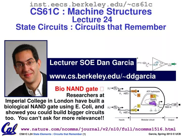
inst.eecs.berkeley.edu /~cs61c CS61C : Machine Structures Lecture 24 State Circuits : Circuits that Remember. Lecturer SOE Dan Garcia www.cs.berkeley.edu/~ddgarcia.

E N D
inst.eecs.berkeley.edu/~cs61cCS61C : Machine StructuresLecture 24 State Circuits : Circuits that Remember Lecturer SOE Dan Garcia www.cs.berkeley.edu/~ddgarcia Bio NAND gate Researchers atImperial College in London have built a biological NAND gate using E. Coli, and showed you could build bigger circuits too. You can’t ask for more relevance!! www.nature.com/ncomms/journal/v2/n10/full/ncomms1516.html
Review • ISA is very important abstraction layer • Contract between HW and SW • Clocks control pulse of our circuits • Voltages are analog, quantized to 0/1 • Circuit delays are fact of life • Two types of circuits: • Stateless Combinational Logic (&,|,~) • State circuits (e.g., registers)
Uses for State Elements • As a place to store values for some indeterminate amount of time: • Register files (like $1-$31 on the MIPS) • Memory (caches, and main memory) • Help control the flow of information between combinational logic blocks. • State elements are used to hold up the movement of information at the inputs to combinational logic blocks and allow for orderly passage.
Accumulator Example Why do we need to control the flow of information? Want: S=0; for (i=0;i<n;i++) S = S + Xi Assume: • Each X value is applied in succession, one per cycle. • After n cycles the sum is present on S.
First try…Does this work? Feedback Nope! Reason #1… What is there to control thenext iteration of the ‘for’ loop? Reason #2… How do we say: ‘S=0’?
Second try…How about this? Roughtiming… Time Register is used to hold up the transfer of data to adder.
Register Details…What’s inside? • n instances of a “Flip-Flop” • Flip-flop name because the output flips and flops between and 0,1 • D is “data”, Q is “output” • Also called “d-type Flip-Flop”
What’s the timing of a Flip-flop? (1/2) • Edge-triggered d-type flip-flop • This one is “positive edge-triggered” • “On the rising edge of the clock, the input d is sampled and transferred to the output. At all other times, the input d is ignored.” • Example waveforms: Fall 2010 -- Lecture #23
What’s the timing of a Flip-flop? (2/2) • Edge-triggered d-type flip-flop • This one is “positive edge-triggered” • “On the rising edge of the clock, the input d is sampled and transferred to the output. At all other times, the input d is ignored.” • Example waveforms (more detail):
Accumulator Revisited (proper timing 1/2) • Reset input to register is used to force it to all zeros (takes priority over D input). • Si-1 holds the result of the ith-1 iteration. • Analyze circuit timing starting at the output of the register.
Accumulator Revisited (proper timing 2/2) • reset signal shown. • Also, in practice X might not arrive to the adder at the same time as Si-1 • Si temporarily is wrong, but register always captures correct value. • In good circuits, instability never happens around rising edge of clk.
Maximum Clock Frequency • What is the maximum frequency of this circuit? Hint… Frequency = 1/Period Max Delay =Setup Time + CLK-to-Q Delay + CL Delay
Pipelining to improve performance (1/2) Extra Register are often added to help speed up the clock rate. Timing… Note: delay of 1 clock cycle from input to output. Clock period limited by propagation delay of adder/shifter.
Pipelining to improve performance (2/2) • Insertion of register allows higher clock frequency. • More outputs per second. Timing…
Recap of Timing Terms • Clock (CLK) - steady square wave that synchronizes system • Setup Time - when the input must be stable before the rising edge of the CLK • Hold Time - when the input must be stable after the rising edge of the CLK • “CLK-to-Q” Delay - how long it takes the output to change, measured from the rising edge of the CLK • Flip-flop - one bit of state that samples every rising edge of the CLK (positive edge-triggered) • Register - several bits of state that samples on rising edge of CLK or on LOAD (positive edge-triggered)
Administrivia • Project 2 Part Two, Due Sunday @23:59:59 • Homework 4 out next will be directly connected to this material! • Please do the reading (in the PDFs) for this material to really understand it!
Finite State Machines (FSM) Introduction • You have seen FSMs in other classes. • Same basic idea. • The function can be represented with a “state transition diagram”. • With combinational logic and registers, any FSM can be implemented in hardware.
Finite State Machine Example: 3 ones… FSM to detect the occurrence of 3 consecutive 1’s in the input. Draw the FSM… Assume state transitions are controlled by the clock: on each clock cycle the machine checks the inputs and moves to a new state and produces a new output…
Hardware Implementation of FSM … Therefore a register is needed to hold the a representation of which state the machine is in. Use a unique bit pattern for each state. + ? = Combinational logic circuit is used to implement a function maps from present state and input to next state and output.
PS Input NS Output 00 0 00 0 00 1 01 0 01 0 00 0 01 1 10 0 10 0 00 0 10 1 00 1 Hardware for FSM: Combinational Logic Next lecture we will discuss the detailed implementation, but for now can look at its functional specification, truth table form. Truth table…
General Model for Synchronous Systems • Collection of CL blocks separated by registers. • Registers may be back-to-back and CL blocks may be back-to-back. • Feedback is optional. • Clock signal(s) connects only to clock input of registers.
Peer Instruction • HW feedback akin to SW recursion • The minimum period of a usable synchronous circuit is at least the CLK-to-Q delay • You can build a FSM to signal when an equal number of 0s and 1s has appeared in the input. 123 a: FFF a: FFT b: FTF b: FTT c: TFF d: TFT d: TTF e: TTT
Peer Instruction Answer • It needs ‘base case’ (reg reset), way to step from i to i+1 (use register + clock).True! • If not, will lose data!True! • How many states would it have? Say it’s n. How does it know when n+1 bits have been seen? • False! • HW feedback akin to SW recursion • The minimum period of a usable synchronous circuit is at least the CLK-to-Q delay • You can build a FSM to signal when an equal number of 0s and 1s has appeared in the input. 123 a: FFF a: FFT b: FTF b: FTT c: TFF d: TFT d: TTF e: TTT
Design Hierarchy system control datapath coderegisters stateregisters combinationallogic multiplexer comparator register logic switchingnetworks
“And In conclusion…” • State elements are used to: • Build memories • Control the flow of information between other state elements and combinational logic • D-flip-flops used to build registers • Clocks tell us when D-flip-flops change • Setup and Hold times important • We pipeline long-delay CL for faster clock • Finite State Machines extremely useful • You’ll see them again 150, 152, 164, 172, …