Download
1 / 1
10 likes | 138 Views
Clock Synchronization & Distribution in VLSI Circuits Project # LH10-MHI. Project Team Principal Investigator Emory W. Zimmers , Jr., PhD Co-PI H. Robert Gustafson, Jr. Graduate Assistant Joshua D. Goldman Graduate Assistant Eric A. Kuijpers

E N D
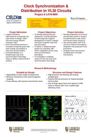
Clock Synchronization & Distribution in VLSI Circuits Project # LH10-MHI Project Team Principal Investigator Emory W. Zimmers, Jr., PhD Co-PI H. Robert Gustafson, Jr. Graduate Assistant Joshua D. Goldman Graduate Assistant Eric A. Kuijpers Undergraduate Assistant Trevor J. Drummond • Project Motivation • Logistics efficiency improvements increasingly rely upon easier to design, faster and more energy efficient computer chips. • One of the primary barriers to increased computing power with lower energy consumption is chip clock synchronization. • Commercialization of a breakthrough chip clock synchronization technology relies on ability to demonstrate it working. • Project Objectives • To develop testing protocols required for commercialization of technology that supports development of easier to design and faster computer chips that use less power. • To deliver a reliable test bed system for evaluating 180-micron integrated circuits using clock synchronization techniques. • To investigate a modeling system for the new chip clock synchronization technology. • Project Activities • Develop proprietary VLSI circuit and test bed system to analyze live performance under active and normal system stressors. • Use testing system with VLSI circuit as a proof-of-concept for integration into production VLSI processors. • Undergo worst-case process modeling prior to foundry manufacture. Research Methodology • Scalable by Design • Applicability to wide range of frequencies. • Minimize interference from electromagnetic coupling. • Prove efficacy with passive transmission lines. • Structure and Design Features • High-precision de-skewing and analog multiplication. • Passive EM transmission for lowest possible intrinsic jitter. • Use of large signal level and rejection of AM noise to reduce jitter from coupled logic switching noise. This project is sponsored (in part) by the National Science Foundation Center for Engineering Logistics and Distribution NSF Award #IIP0434210