Download
1 / 13
130 likes | 306 Views
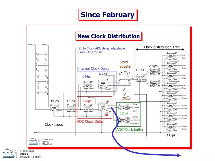
Since February. Clock Driver Needed Improvement. Original Version. ADC Clock outputs slow due to level shifter. Level Shifter. Buffer. Improved Version. V EE Routing Optimization. V EE ~ 5 mV. DELAY. GAIN BITS PIPELINE +OUTPUT. CLOCK I/O. V EED pad. COMMAND DECODER.

E N D
Original Version ADC Clock outputs slow due to level shifter Level Shifter Buffer
VEE Routing Optimization VEE ~ 5 mV DELAY GAIN BITS PIPELINE +OUTPUT CLOCK I/O VEED pad COMMAND DECODER
Digital Bias Distribution I I’ VBIAS~0 VEE VEE’
Timing Fixed Delay S/H (Internal clocks) CKi Variable Delay CKAD (to ADC) Input clock (CKi) is the “observable” All subsequent timings relative to CKi
T/H Timing CK H = 8.5 ns CKi S/H FPUout
Timing Relations N+1 N+2 N+3 N+4 N Signal CKi S S/H H CKAD N-3 N-2 N-1 N ADC N-3 N-2 N-1 N FPUo
FPU Output Bit Timing CK FPo = 14.2 ns S/H FPo = 5.7 ns 2.5 pipeline delays
Timing Diagram N Signal CKi S S/H H 8.5 ns CKAD 8.9 ns 9 typ ns N-3 N-2 ADC N-3 N-2 FPUo 14.2 ns