Download
1 / 27
270 likes | 458 Views
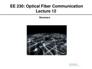
EE 230: Optical Fiber Communication Lecture 12. Receivers. From the movie Warriors of the Net. Receiver Functional Block Diagram. Fiber-Optic Communications Technology-Mynbaev & Scheiner. Receiver Types. Low Impedance Low Sensitivity Easily Made Wide Band. High Impedance

E N D
EE 230: Optical Fiber Communication Lecture 12 Receivers From the movie Warriors of the Net
Receiver Functional Block Diagram Fiber-Optic Communications Technology-Mynbaev & Scheiner
Receiver Types Low Impedance Low Sensitivity Easily Made Wide Band High Impedance Requires Equalizer for high BW High Sensitivity Low Dynamic Range Careful Equalizer Placement Required Transimpedance High Dynamic Range High Sensitivity Stability Problems Difficult to equalize
Equivalent Circuits of an Optical Receiver High Impedance Design Transimpedance Design Transimpedance with Automatic Gain Control Fiber-Optic Communications Technology-Mynbaev & Scheiner
Receiver Noise Sources • Photon Noise • Also called shot noise or Quantum noise, described by poisson statistics • Photoelectron Noise • Randomness of photodetection process leads to noise • Gain Noise • eg. gain process in APDs or EDFAs is noisy • Receiver Circuit noise • Resistors and transistors in the the electrical amplifier contribute to circuit noise Photodetector without gain Photodetector with gain (APD)
Noise Power Frequency Noise Power Frequency 1/f noise Noise Power Fc Frequency Noise Johnson noise (Gaussian and white) Shot noise (Gaussian and white) “1/f” noise
Johnson (thermal) Noise Noise in a resistor can be modeled as due to a noiseless resistor in parallel with a noise current source
Photodetection noise The electric current in a photodetector circuit is composed of a superposition of the electrical pulses associated with each photoelectron The variation of this current is called shot noise Noise in photodetector If the photoelectrons are multiplied by a gain mechanism then variations in the gain mechanism give rise to an additional variation in the current pulses. This variation provides an additional source of noise, gain noise Noise in APD
Signal to Noise Ratio Signal to noise Ratio (SNR) as a function of the average number of photo electrons per receiver resolution time for a photo diode receiver at two different values of the circuit noise Signal to noise Ratio (SNR) as a function of the average number of photoelectrons per receiver resolution time for a photo diode receiver and an APD receiver with mean gain G=100 and an excess noise factor F=2 At low photon fluxes the APD receiver has a better SNR. At high fluxes the photodiode receiver has lower noise
Dependence of SNR on APD Gain Curves are parameterized by k, the ionization ratio between holes and electrons Plotted for an average detected photon flux of 1000 and constant circuit noise
Receiver SNR vs Bandwidth Double logarithmic plot showing the receiver bandwidth dependence of the SNR for a number of different amplifier types
Basic Feedback Configuration Ii Is A Vi + Ro Is If Ri - Parallel Current Feedback Lowers Input Impedance Parallel Voltage Sense: Voltage Measured and held Constant => Low Output Impedance bVo Stabilizes Transimpedance Gain Ii ZtIi + Zo Zi -
Transimpedance Amplifier Design i + Output Voltage Proportional to Input current Z i - Zero Input Impedance Vi A Vi + Ro Ri - Typical amplifier model With generalized input impedance And Thevenin equivalent output + A Vi + Ro is Vo Vi Ri - - Calculation of Openloop transimpedance gain: Rm
Vcc1 Vcc2 Controls open loop gain of amplifier, Reduce to decrease “peaking” Rc Q2 Q1 Out Rf Photodiode Most Common Topology Has good bandwidth and dynamic Range Vbias Transimpedance approximately equals Rf low values increase peaking and bandwidth Transimpedance Amplifier Design Example See Das et. al. Journal of Lightwave Technology Vol. 13, No. 9, Sept.. 1995 For an analytic treatment of the design of maximally flat high sensitivity transimpedance amplifiers
Bit Error Rate BER is equal to number of errors divided by total number of pulses (ones and zeros). Total number of pulses is bit rate B times time interval. BER is thus not really a rate, but a unitless probability.
BER vs. Q, continued When off = on and Voff=0 so that Vth=V/2, then Q=V/2. In this case,
Sensitivity The minimum optical power that still gives a bit error rate of 10-9 or below
Receiver Sensitivity (Smith and Personick 1982)
Maximum Signal Level Input Optical Power Dynamic Range receiver Sensitivity High Rf (High Impedance Preamplifier) Feedback Resistance Low Rf (Transimpedance Preamplifier Patten Generator Transmitter Adjustable Attenuator Optical Receiver Bit Error Rate Counter Optional Clock Dynamic Range and Sensitivity Measurement Dynamic range is the Optical power difference in dB over which the BER remains within specified limits (Typically 10-9/sec) The low power limit is determined by the preamplifier sensitivity The high power limit is determined by the non-linearity and gain compression Experimental Setup
Eye Diagrams Transmitter “eye” mask determination Formation of eye diagram Eye diagram degradations Computer Simulation of a distorted eye diagram Fiber-Optic Communications Technology-Mynbaev & Scheiner
Power Penalties • Extinction ratio • Intensity noise • Timing jitter
Extinction ratio penalty Extinction ratio rex=P0/P1
Intensity noise penalty rI=inverse of SNR of transmitted light
Timing jitter penalty Parameter B=fraction of bit period over which apparent clock time varies