Download
1 / 17
190 likes | 375 Views
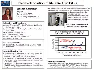
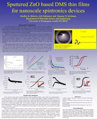
Identification of Defects and Secondary Phases in Reactively Sputtered Cu 2 ZnSnS 4 Thin Films. Vardaan Chawla , Stacey Bent, Bruce Clemens April 7 th , 2010 Center on Nanostructuring for Efficient Energy Conversion Materials Science and Engineering Stanford University. Outline. Motivation

E N D
Identification of Defects and Secondary Phases in Reactively Sputtered Cu2ZnSnS4 Thin Films VardaanChawla, Stacey Bent, Bruce Clemens April 7th, 2010 Center on Nanostructuring for Efficient Energy Conversion Materials Science and Engineering Stanford University
Outline • Motivation • Problems with characterization of thin films • Experimental approach • Results • X-ray diffraction • Raman Spectroscopy • Transmission Electron Microscopy • Scanning Auger Microscopy • Summary & Acknowledgements
Motivation – Phase Equilibrium SnS2 Ternary Phase Diagram Binary Phase Diagram Cu2SnS3 CZTS Cu2S ZnS • CZTS is a line compound between Cu2SnS3 and ZnS • Theoretically even a 2-3% compositional variation could lead to phase separation Olekseyuk, I.D. "Phase Equilibria in the Cu2S-ZnS-SnS2 System." Journal of Alloys and Compounds. 368. (2004): 135-143. Print.
Motivation – Crystal Structure Theoretical XRD Patterns of CZTS, Cu2SnS3, and ZnS • Crystal structures of secondary phases similar to CZTS • All primary peaks overlap and hard to separate • Low intensity peaks cannot be seen easily in thin films
H2S H2S H2S H2S H2S H2S 4H2S + 2Cu + Zn + Sn Cu2ZnSnS4 + 4H2 CZTS Experimental Approach ReactiveSputtering Zn Cu Sn Substrate • Introduce H2S into chamber during sputter deposition • Sulfur is incorporated into the film in one step (no anneal) • Expect to see higher densities and improved film quality
Characterization - XRD Varying Zn/(Cu+Sn) Ratio (112) SnS2 Cu2SnS3 (220) (101) (312) (200) Cu2S ZnS • Zn/(Cu+Sn) ratio is varied while holding Cu/Sn ratio constant • Impossible to determine difference between CZTS, CTS, and ZnS from XRD pattern Olekseyuk, I.D. "Phase Equilibria in the Cu2S-ZnS-SnS2 System." Journal of Alloys and Compounds. 368. (2004): 135-143. Print.
Characterization - XRD Varying Cu/(Zn+Sn) Ratio (112) SnS2 (200) (220) Cu2SnS3 (312) (101) Cu2S ZnS CuS Cu2S • Cu/(Zn+Sn) ratio is varied while holding Zn/Sn ratio constant • Need to get very far off 2:1:1 stoichiometry before any CuxS phases can be seen • CuxS can be removed with KCN etch Olekseyuk, I.D. "Phase Equilibria in the Cu2S-ZnS-SnS2 System." Journal of Alloys and Compounds. 368. (2004): 135-143. Print.
Characterization – Raman Varying Zn/(Cu+Sn) Ratio Varying Cu/(Zn+Sn) Ratio • Raman spectra show only minor changes even though composition is varied dramatically • No evidence of the CuxS phase shown by other groups at growth temperatures higher than 500C
Device Fabrication CZTS Device Stack SEM Image Aluminum Grid 340 nm ZnO:Al (n-type) ZnO:Al ZnO ZnO 85 nm CdS 55 nm CdS(n-type) CZTS Absorber (p-type) 1.75 µm CZTS Molybdenum Layer 1 µm Glass Substrate 3000 µm 500nm Mo • Zn-rich films incorporated into standard CIGS device stack for testing
Device Characterization I-V Measurement EQE Measurement • First CZTS devices grown by a reactive sputtering process • Efficiency = 1.35% • Degraded EQE clearly points to undetected defects in the absorber
Characterization - TEM CZTS • Detrimental secondary phase interspersed in CZTS matrix • Stacking faults in the secondary phase point to a transition between cubic and hexagonal crystal structures Second phase CZTS 500nm Second phase 5nm 200nm
Characterization - Auger Cu CZTS ZnS Zn 2 um • Raster beam over sputtered surface of sample and scan for Cu, Zn, Sn • Overlay Cu, Zn, Sn signal • Composition variation points to CZTS / ZnS (Zn-rich) Sn
Characterization - CdZnS CdS – ZnS Phase Diagram XRD before and after CBD (112) H H-ZnS C + H (220) (312) (101) C • Cd penetration into ZnS lowers the cubic-hexagonal transition temperature • Stacking faults in TEM images are created during CBD of CdS layer Chen et al.“Solid State Phase Equilibria in the ZnS-CdS System." Materials Research Bulletin. 23. (1988): 1667-1673. Print.
Characterization - Auger CZTS Sn CdZnS 2 um Cd • Overlay Sn and Cd signal • Cd ion exchanges with Zn during bath deposition and penetrates the ZnS phase
Summary • CZTS thin films were grown using Reactive Sputtering • Films were characterized using X-ray Diffraction and Raman Spectroscopy • Full devices have been grown and tested but are limited due to secondary phases in the films • Transmission Electron Microscopy and Scanning Auger Microscopy can be used to identify these secondary phases
Acknowledgements • US Department of Energy, Office of Basic Energy Sciences as part of an Energy Frontier Research Center • http://www.er.doe.gov/bes/EFRC/index.html • Applied Quantum Technologies • Local thin film solar startup • http://www.aqtsolar.com
Questions Questions?