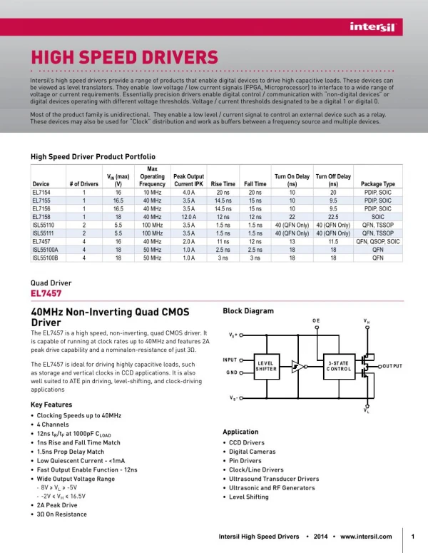
High Speed Logic
High Speed Logic. Power supply systems. Part 1. High speed circuit. 0.1 Frequency / time relation. Basic facts and tools for the analysis of the edge of a clock Rise time (T r ) = time to rise from 10% to 90% of the signal. V. 90%. 10%. t. Tr. A fast falling edge. A slow rising edge.

High Speed Logic
E N D
Presentation Transcript
High Speed Logic Power supply systems power supply systems (v3a)
Part 1 High speed circuit power supply systems (v3a)
0.1 Frequency / time relation • Basic facts and tools for the analysis of the edge of a clock • Rise time (Tr) = time to rise from 10% to 90% of the signal. V 90% 10% t Tr A fast falling edge A slow rising edge power supply systems (v3a)
0.1 Knee frequency calculationConvert rise-time edge (Tr) and frequency (Fknee) • Fknee=0.5/Tr • e.g. edge=5ns, what is the equivalent frequency. • Fknee==0.5/5ns=100MHz. Period/2=Tr Period of the equivalent signal power supply systems (v3a)
Analog / digital signal relation • Can a digital signal pass an analog circuit without distortion? • Use Fknee to quickly estimate if the signal can pass the clock edge or not. power supply systems (v3a)
Short term (edge) response by F_knee method Rising or falling edge= short term behavior Level 1 or 0 = long term behavior power supply systems (v3a)
Short term (edge) response by F_knee • At high frequency, a wire becomes an inductor. Then a high frequency signal (fast edge) is attenuated (or distorted). • F_knee0.5/Tr , where Tr= rise time I R L A long wire or PCB trace power supply systems (v3a)
Frequency response of a low pass trace • Shorter rise time pushes frequency requirement higher. Important results: • (1) A circuit has flat frequency response up to and including F_knee (0.5/Tr) will pass the digital signal with rise edge (Tr). • (2) The behavior above F_knee of a digital circuit will have little effect on how it processes digital signals. • (3) Frequency lower than F_knee will affect the long term behavior of the signal. power supply systems (v3a)
How to apply the F_knee technique • Find or estimate Tr rise time of your signal. • Find F_knee 0.5/Tr • Now whether your circuit can pass this signal or not depends on whether the circuit has flat frequency up to F_knee or not. power supply systems (v3a)
Example • Since F_knee =0.5/Tr, Tr=0.5/100MHz • Hence Tr should not be shorter than 5ns. • What would happen if Tr is shorter than 5NS (e.g. 3ns) ? Answer: distorted, edge smoothed This circuit has flat frequency response up to 100MHZ 5ns 5ns A PCB TRACE The output of a 3ns edge 3ns 5ns power supply systems (v3a)
F_knee method is only an approximation • F_knee is only defined by the signal rise time and has no relation to other frequency domain parameters. It is easy to use and remember. • An imprecise measure of spectral contents, it cannot make precise prediction of circuit behavior. • Use Fourier transform if an accurate result is required. power supply systems (v3a)
Power exercise 0.1 • A circuit can pass signals of 200 MHz without distortion, what is the shortest rising edge that can pass this circuit? power supply systems (v3a)
0.2 The horror of large dI/dt • Since V =-L dI/dt , L=inductance. • Since the traces are inductive, Large dI/dt will create huge noise voltage V in the circuit. dI/dt V LargedI/dt creates large voltage V here power supply systems (v3a)
Speed dI/dt problem • Logic families having minimum switch times much faster than the propagation delay suffer an unnecessary penalty in system design. Large dI/dt creates problems. • Given two families with identical propagation delay statistics, the family with the slowest output switching time will be cheaper and easier to run. power supply systems (v3a)
Speed dV/dt problems • Circuit response lower than Fknee may distort signal, circuit response higher than Fknee is not important in our design. • Shorter Tr (switch time) results in higher Fknee. So unnecessary short Tr is a problem. • So shorter Tr will not work in poorly designed circuits. • Shorter Tr will give larger dI/dt, which will cause ground bounce. (will be discussed later) power supply systems (v3a)
How to find dI/dt from dV/dt • dI/dt creates problems. • Since dV/dt is easier to measure, so we try to find dI/dt fromV (output voltage change),Tr(rise time) and C(load capacitance). • We will show that • max(dI/dt) =1.52 V C/(Tr)2 power supply systems (v3a)
T10-90=Tr =rise time from 10 to 86 % Fig.2.14 of [1] Max slope is (V/2)/(Tr/2) = V/Tr Max slope is (V/Tr)/ (Tr/2)] =2 V/(T2r )---(i) ------------------------- More precisely: consider voltage difference 0.76*V (from 10 % to 86%) in equ. (i). Max slope is =0.75*{2 V/(Tr2)} 1.52 V/(T2r ) Tr/2 power supply systems (v3a)
Showed two important relations • (1/R)max(dV/dt)= (1/R)V/Tr • C*max(d2V/dt2)=C*1.52*V/(Tr)2 power supply systems (v3a)
VL Power supply V L C R Tr Effect of dI/dt at output and at power supply is similardI/dt is difficult to measure, so use dV/dt easier estimate, it is easier • to 1/T2r, big • more significant 1/Tr, smaller so ignored power supply systems (v3a)
L R Tr Max(dIcapacitor/dt) 1/T10-902Shorter Tr will give larger dI/dt, which will cause ground bounce. VL Power supply Same dI/dt dI/dt C power supply systems (v3a)
VL Power supply V L C R Tr Exercise 0.2 5V step 1ns power supply systems (v3a)
Part 2 Power systems power supply systems (v3a)
Power system • Fixed and variable power supply • use 78xx chip • Use power transistor 3055 • Use of opto-coupler • Use capacitors to stabilize power power supply systems (v3a)
1 3 Fixed at 5V, current limit 500mA 7805 7V or above 200uF 2 TIP3055 Input power V1(5V) R1 R2 100uF Fixed and variable Power supply http://eddie.dyec.com.tw/diy-demo/audio-diy/cd_dvd_modify/cd-100_2/cd100_2image/7805.jpg • Use power supply chips 78xx • E.g. 7805 for supper isolation to reduce interference • E.g. Variable power supply design and usage, e.g. step down 5V --> 3V. Output=V1[R2/(R1+R2)] (0-5V) power supply systems (v3a)
TIP3055 R1 Input power V1 Output=V1[R2/(R1+R2)] R2 Power exercise 1 • If I have a power source 9 V and want to produce a power supply of 5V, R1=10K. • Suggest two methods to achieve this. • Answer: power supply systems (v3a)
Example: Use of 7805 power stabilizer and opto isolator 8031 7.2V or above Power supply 7805 7805 Xilinx Optical Isolators 4N35 2 systems has no electrical linkage light Electrically Isolated Low power High power 3 Volts battery Current driver circuit Left/Right motors power supply systems (v3a)
Board level Power supply sys. • Power systems • provide stable voltage references • distribute power to all devices • We will learn about how to find • board level bypass capacitors • capacitor array • Examples and pictures are from Reference :High speed digital design by HW Johnson and Graham, Prentice Hall power supply systems (v3a)
Method (in single ended signaling) to reduce ground noise (low cost) for normal gates : return current is the same as the ground • Use better power distribution method: • Rule 1: Low impedance ground • Rule 2: Low impedance power (5V) lines • Rule 3:Low impedance between power (5V) and ground (0V) -- use of bypass capacitors. power supply systems (v3a)
Power Rule 1: Use low-impedance ground connections between gates -- use ground planes, power rails. • Reasons: • Fig. 8.2 shows the hypothetical noise “N” in the ground loop, which is caused by the return current flowing through the ground inductance power supply systems (v3a)
Power Rule 2: The impedance between power pins on the two gates should be as low as possible (fig. 8.3) --use power planes,etc. Reasons: • common path inductance between power pins on any other gates is a problem even the ground is perfect. • If N is large, gate A may receive a lower power supply or reference voltage. power supply systems (v3a)
Power Rule 3: There must be a low-impedance path between power and ground (fig. 8.4)-- use by- pass-capacitors. • Reasons (Fig 8.3): • The return current flows thru. the battery should create a voltage drop as low as possible to maintain a good reference. The impedance of the battery must be low. • By pass capacitors provide such low impedance paths. Lpcable=100nH Ltot=N number of LC3 in parallel C3 C3 Perfect Power supply Cap. array LC2 Board bypass capacitor C2 C3 power supply systems (v3a)
Use of power, ground planes and capacitor array Rule3 Rule 2 Rule1 power supply systems (v3a)
Power system design techniques:Multi-layer Power distribution • Power supplies designed and sold usually have very low output impedance. • But the wiring to the board and devices may contain inductance. • To maintain a stable power to the circuits we have to solve it in 3 different levels: • Power distribution wiring • Board level filtering • Local filtering at individual integrated circuits power supply systems (v3a)
Level 1: Power distribution wiring • Resistance of power distribution wiring. • Resistance proportional to inverse diameter wire, 40% increase of wire diameter reduces resistance by 1/2. • Sense wire in new power supply designs corrects for resistance in power distribution wiring ( http://reprap.org/bin/view/Main/PCPowerSupply) • Inductance, a more difficult issue. (Section 8.2.1) • Use low-inductance wiring -- wide-flat wires. • Use differential logic Fig. 8.6 (not economical) • Reduce power supply current change can minimize the effect of inductance -- using by pass capacitors. power supply systems (v3a)
Level 2 :Board level filtering • Fig. 8.7, switching at output of gate A can create a large current change through the power supply. • For a 1ns edge (at high frequency) , the inductance blocks the current from the power supply to gate A. • Add C2 (board level by pass capacitor) in fig. 8.8 to reduce the current passing through the inductance. • Example 8.1 shows how to calculate the value of the board level by pass capacitor. This capacitor Cboard_bypass provides low impedance up to a Power-System-Wiring frequency FPSW. Water tanks In Germany Mannheim power supply systems (v3a)
By-pass capacitor 10uF Demo + • Youtube TX (Clean) Vcc (Clean) TX (Noisy) Vcc (Noisy) using by-pass capacitor No by-pass capacitor power supply systems (v3a)
A PC mother board with board level by-pass filter (use parallel capacitors to make a big one: reduce leg inductance; save size and cost) Board level by-pass capacitors(C2) Power supply and cable power supply systems (v3a)
C2 to be added power supply systems (v3a)
Level 3: Local filtering at individual integrated circuits • However no capacitor is perfect, LC2 (at the legs of by pass capacitor C2)may cause its impedance to rise at high frequency. • The best way to get very low inductance is to use a lot of parallel small capacitors. • Use capacitor array to reduce the the problem of LC2 at high frequency. • See Example 8.2 power supply systems (v3a)
Analogouswater delivery system or power supply systems (v3a)
Multi-level by pass capacitors design • Power supply -> board --> individual Ics • Example:Fpsw Fboard Fc_array • below159KHz 159K->3.18M 3.18M->Fknee • 10u-1000uF 32x0.016uF • A power supply provides low impedance at low frequency. • Board level by pass capacitors provide low impedance at higher frequency • Parallel a lot of small capacitors provide very low impedance up to a very high frequency Fknee(e.g. edge=5ns, Fknee=0.5/Tr=0.5/5ns=100MHz). power supply systems (v3a)
Power supply bypass capacitor design • Design calculations, find power supply systems (v3a)
Revision of important formulas(Remember them!!!!) • Impedance of C at freq. F=Xc=1/2 F C • Impedance of L at freq. F=XL=2 F L • I=C(dV/dt) current passing through a capacitor with changing voltage • V=L(dI/dt) voltage across an inductor with changing current • Also when impedance is in terms of Fknee: • Fknee=0.5/Tr • Xc=1/ 2 Fknee C=Tr/ C • XL=2 Fknee L= L/Tr power supply systems (v3a)
Level 1 - Power distribution lines • Board level by pass capacitor(C2) design Cap array(C3) 0.1 ~ 1uF Vcc Power supply Ground Board level electrolytic bypass capacitor 10~500uF Digital circuit board power supply systems (v3a)
Level 2 - bypass capacitor design • Board level by pass capacitor (C2) design Cap array (c3) 0.1 ~ 1uF Vcc Power supply Ground Board level electrolytic bypass capacitor 10~500uF Digital circuit board power supply systems (v3a)
Capacitor array C3 (a number of surface mounted capacitors) Old type power supply systems (v3a)
Capacitor array C3 (a number of new type surface mounted capacitors) Old type power supply systems (v3a)
Board level filtering calculationsWhy board level by-pass cap. C2 is needed? • L=100 nH, V =5V, Cload=50pF, Tr=5ns • (dI/dt) max =1.52 V C1/Tr2=1.5x107A/s • L(dI/dt)max=1.5x107x100x10-9=1.5Volts(large!) • the voltage across the inductor is too high. power supply systems (v3a)
Procedure for level 2 (board level) calculation • 2-1. First find out the maximum change of current the circuit demands. • 2-2. Then find the maximum tolerated impedance of the inductor • 2-3. Find at what signal frequency (or edge using Tr=0.5/Fknee) this inductor has too much impedance • 2-4. Find the value of the required bypass cap. C2 power supply systems (v3a)
Maximum noise allowed=0.1V Perfect 5V power supply Digital circuit, when 100 gates are switching draws 1A Lpcable=100nH impedance<0.1 Ground Given:N=100 gates, C=10pF load in t =5ns, supply voltage= E,inductance Lpcable= 100nH • Step2-1: find max. change of current the circuit demands • Assume max. tolerable noise EN=0.1Volts • I=Call(dV/dt)=NC E/ t = 100•10pF •5V/5ns=1A power supply systems (v3a)