Download
1 / 11
110 likes | 229 Views
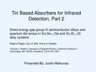
Tin Based Absorbers for Infrared Detection, Part 2. Direct energy gap group IV semiconductor alloys and quantum dot arrays in Sn x Ge 1-x /Ge and Sn x Si 1-x /Si alloy systems Regina Ragan, Kyu S. Min, Harry A. Atwater

E N D
Tin Based Absorbers for Infrared Detection, Part 2 Direct energy gap group IV semiconductor alloys and quantum dot arrays in SnxGe1-x/Ge and SnxSi1-x/Si alloy systems Regina Ragan, Kyu S. Min, Harry A. Atwater Thomas J. Watson Laboratory of Applied Physics, California Institute of Technology, MS 128-95, Pasadena, CA 91125, USA Presented By: Justin Markunas
Recap • Attempting to use a-phase tin for IR detection • Bandgap separation achieved by growing a thin film layer • a-phase/b-phase transition temperature raised by pseudomorphic epitaxial growth • For necessary absorption and correct bandgap, superlattices required • Both CdTe and InSb failed as superlattice materials with a-phase tin(lattice matched materials)
Si Read-Out Circuitry HgCdTe Detector Array CdZnTe Substrate Si1-xSnx Alloys • Motivations: • Many advantages of growing on a silicon substrate • Cost considerations • Thermally compatible to read-out circuitry Contact Metallization In Bump Bond • Si1-xSnx predicted to become direct bandgap for x > .9
Si1-xSnx Alloys • Drawbacks: • Mismatch between Si and Sn is large (aSi= 5.43 Å aSn= 6.48 Å) • 19.5% mismatch • Makes pseudomorphic growth nearly impossible • Solubility of Sn in Si is low (~5x1019 cm-3) • Results in an x-value ~.01 • This changes Si electronic band structure very little • Surface segregation occurs under normal MBE growth conditions
Si Cap Layer: 14nm Si1-xSnx: 1-4nm Si Buffer Layer Si Substrate Si Cap Layer: 14nm Sn quantum dots Si Buffer Layer Si Substrate Si1-xSnx Quantum Dots • Solution: • Grow thin Si1-xSnx layers on Si by MBE (1-4 nm thick) • Attempted x-values: .05 - .2 • Growth performed at 170°C • Anneal sample at 500 – 800°C • Si1-xSnx layer segregates and forms Sn quantum dots • Quantum confinement effects of dots create a nonzero Sn bandgap Anneal
TEM Analysis • Cross-sectional bright field TEM images shown • 2nm thick Si.95Sn.05 layer • Annealed at 800°C for 30 minutes
TEM Analysis • Plan-view bright field TEM images shown • 2nm thick Si.9Sn.1 layer • One sample annealed at 500°C for 3 hours • Another at 800°C for 30 minutes • Results: • Phase separation evident in as-grown film • Sample annealed at 500°C shows formation of quantum dots with gradually varying background contrast • Sample annealed at 800°C results in larger dots with little variation in background contrast • RBS Result: • Dot composition was estimated to be pure Sn
IR Absorption • Key unknown: • Which allotrope of Sn the dots are composed of • Can determine by taking IR absorption spectrum • Measurement Setup: • Shape sample into a trapezoid • Measurement taken by a FTIR spectrometer • Incident radiation at angle q>qc • Number of passes through Sn layer:
IR Absorption • Results from a 2nm Si.9Sn.1 sample : • Eg ~ .27eV • Absorption doubles after annealing the sample at 800°C • Absorption is consistent with direct interband transitions
Dot Growth • Measurement: • Anneal a Si1-xSnx sample at 650°C and plot dot size as time elapses • Results: • Dots trend to larger sizes and lower density as time progresses • Growth Mechanisms: • Before annealing: decomposition of Si1-xSnx and nucleation of Sn nanocrystals • After annealing: coarsening occurs, where larger dots grown at the expense of smaller ones
Conclusions • Sn quantum dots in Si have been fabricated and shown to absorb IR radiation • Bandgap adjusted by controlling dot size • Still many issues to resolve before making a detector • Dot size controllability • Doping • Absorber thickness